FDC658AP Fairchild Optoelectronics Group, FDC658AP Datasheet
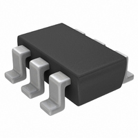
MOSFET P-CH SGL LL 30V 4A SSOT6

FDC658AP

Manufacturer Part Number
FDC658AP
Description
MOSFET P-CH SGL LL 30V 4A SSOT6
Manufacturer
Fairchild Optoelectronics Group
Series
PowerTrench®r
Datasheet

Specifications of FDC658AP

Fet Type
MOSFET P-Channel, Metal Oxide
Fet Feature
Logic Level Gate
Rds On (max) @ Id, Vgs
50 mOhm @ 4A, 10V
Drain To Source Voltage (vdss)
30V
Current - Continuous Drain (id) @ 25° C
4A
Vgs(th) (max) @ Id
3V @ 250µA
Gate Charge (qg) @ Vgs
8.1nC @ 5V
Input Capacitance (ciss) @ Vds
470pF @ 15V
Power - Max
800mW
Mounting Type
Surface Mount
Package / Case
SuperSOT-6
Lead Free Status / RoHS Status
Lead free / RoHS Compliant
Other names
FDC658APTR

Available stocks

Company
Part Number
Manufacturer
Quantity
Price
Part Number:
FDC658AP
Manufacturer:
Fairchild Semiconductor
Quantity:
140 672
Part Number:
FDC658AP
Manufacturer:
FAIRCHILD
Quantity:
8 000
Part Number:
FDC658AP
Manufacturer:
FAIRCHILD/仙童
Quantity:
20 000
Part Number:
FDC658AP
0
Company:
Part Number:
FDC658AP
Quantity:
84 579
Company:
Part Number:
FDC658AP
Quantity:
90
Company:
Part Number:
FDC658AP
Quantity:
6 000
Part Number:
FDC658AP-NL
Manufacturer:
FAIRCHILD/仙童
Quantity:
20 000
©2006 Fairchild Semiconductor Corporation
FDC658AP Rev. B (W)
Absolute Maximum Ratings
Thermal Characteristics
Package Marking and Ordering Information
FDC658AP
Single P-Channel Logic Level PowerTrench
-30V, -4A, 50mΩ
General Description
This P-Channel Logic Level MOSFET is produced using
Fairchild's advanced PowerTrench process. It has been
optimized for battery power management applications.
Applications
V
V
I
P
T
R
R
D
J
DS
GS
D
θJA
θJC
Battery management
Load switch
Battery protection
DC/DC conversion
Symbol
, T
Device Marking
STG
.58A
Drain-Source Voltage
Gate-Source Voltage
Drain Current - Continuous
Maximum Power dissipation
Operating and Storage Junction Temperature Range
Thermal Resistance, Junction-to-Ambient
Thermal Resistance, Junction-to-Case
PIN 1
D
SuperSOT
D
- Pulsed
FDC658AP
Device
S
D
D
TM
Parameter
T
-6
G
A
= 25°C unless otherwise noted
Reel Size
7inch
1
Features
Max r
Max r
Low Gate Charge
High performance trench technology for extremely low
r
RoHS Compliant
DS(on)
DS(on)
DS(on)
Tape Width
(Note 1a)
(Note 1a)
(Note 1b)
(Note 1a)
(Note 1)
®
8mm
= 50 mΩ @ V
= 75 mΩ @ V
MOSFET
1
2
3
GS
GS
-55 to +150
Ratings
= -10 V, I
= -4.5 V, I
±25
-30
-20
1.6
0.8
78
30
-4
3000 units
6
Quantity
5
4
January 2006
www.fairchildsemi.com
D
D
= -4A
= -3.4A
Units
°C/W
°C/W
°C
W
V
V
A

Related parts for FDC658AP

FDC658AP Summary of contents

Page 1

... Thermal Resistance, Junction-to-Ambient θJA R Thermal Resistance, Junction-to-Case θJC Package Marking and Ordering Information Device Marking Device .58A FDC658AP ©2006 Fairchild Semiconductor Corporation FDC658AP Rev. B (W) Features Max r DS(on) Max r DS(on) Low Gate Charge High performance trench technology for extremely low r DS(on) RoHS Compliant ...

Page 2

... R is guaranteed by design while R θ C/W when mounted Scale letter size paper 2: Pulse Test: Pulse Width < 300 µs, Duty Cycle < 2.0% FDC658AP Rev 25°C unless otherwise noted J Test Conditions I = -250µ -250µA, D Referenced to 25° ...

Page 3

... GS 1.4 1.2 1 0.8 0.6 -50 - JUNCTION TEMPERATURE ( J Figure 3. Normalized On-Resistance vs Junction Temperature - GATE TO SOURCE VOLTAGE (V) GS Figure 5. Transfer Characteristics FDC658AP Rev. B (W) 2 1.8 -4.0V 1.6 1.4 -3.5V 1.2 -3. Figure 2. 0.22 0.18 0.14 0.1 T 0.06 0.02 75 100 125 150 Figure ...

Page 4

... SINGLE PULSE 0.001 0.00001 0.0001 Figure 11. Thermal characterization performed using the conditions described in Note 1b. Transient thermal response will change depending on the circuit board design. FDC658AP Rev. B (W) 600 V = -5V DS -10V 450 -15V 300 150 Figure 8 ...

Page 5

TRADEMARKS The following are registered and unregistered trademarks Fairchild Semiconductor owns or is authorized to use and is not intended exhaustive list of all such trademarks. FAST ® ACEx™ ActiveArray™ FASTr™ Bottomless™ FPS™ Build it Now™ FRFET™ ...

Related keywords