STW34NB20 STMicroelectronics, STW34NB20 Datasheet - Page 2
STW34NB20
Manufacturer Part Number
STW34NB20
Description
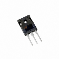
MOSFET N-CH 200V 34A TO-247
Manufacturer
STMicroelectronics
Series
PowerMESH™r
Specifications of STW34NB20
Fet Type
MOSFET N-Channel, Metal Oxide
Fet Feature
Standard
Rds On (max) @ Id, Vgs
75 mOhm @ 17A, 10V
Drain To Source Voltage (vdss)
200V
Current - Continuous Drain (id) @ 25° C
34A
Vgs(th) (max) @ Id
5V @ 250µA
Gate Charge (qg) @ Vgs
80nC @ 10V
Input Capacitance (ciss) @ Vds
3300pF @ 25V
Power - Max
180W
Mounting Type
Through Hole
Package / Case
TO-247-3
Configuration
Single
Transistor Polarity
N-Channel
Resistance Drain-source Rds (on)
0.075 Ohm @ 10 V
Forward Transconductance Gfs (max / Min)
17 S
Drain-source Breakdown Voltage
200 V
Gate-source Breakdown Voltage
+/- 30 V
Continuous Drain Current
34 A
Power Dissipation
180000 mW
Maximum Operating Temperature
+ 150 C
Mounting Style
Through Hole
Minimum Operating Temperature
- 65 C
Current, Drain
34 A
Gate Charge, Total
60 nC
Package Type
TO-247
Polarization
N-Channel
Resistance, Drain To Source On
0.062 Ohm
Temperature, Operating, Maximum
+150 °C
Time, Turn-off Delay
17 ns
Time, Turn-on Delay
30 ns
Transconductance, Forward
17 S
Voltage, Breakdown, Drain To Source
200 V
Voltage, Forward, Diode
1.5 V
Voltage, Gate To Source
±30 V
Lead Free Status / RoHS Status
Lead free / RoHS Compliant
Other names
497-2659-5
Available stocks
Company
Part Number
Manufacturer
Quantity
Price
Company:

Part Number:
STW34NB20
Manufacturer:
ST
Quantity:
15 000
Company:
Part Number:
STW34NB20
Manufacturer:
IXYS
Quantity:
5 000


STW34NB20
Table 3. Absolute Maximum Ratings
Note: 1. Pulse width limited by safe operating area
Table 4. Thermal Data
Table 5. Avalanche Characteristics
2/10
Symbol
Symbol
R
R
Symbol
I
V
DM
thj-case
V
V
thj-amb
P
T
E
DGR
I
I
I
T
T
GS
DS
stg
AR
D
D
tot
AS
j
l
(1)
Drain-source Voltage (V
Drain- gate Voltage (R
Gate-source Voltage
Drain Current (cont.) at T
Drain Current (cont.) at T
Drain Current (pulsed)
Total Dissipation at T
Derating Factor
Storage Temperature
Max. Operating Junction Temperature
Thermal Resistance Junction-case
Thermal Resistance Junction-ambient
Maximum Lead Temperature For Soldering Purpose
Avalanche Current, Repetitive or Not-Repetitive
(pulse width limited by T
Single Pulse Avalanche Energy
(starting T
j
= 25 °C; I
Parameter
Parameter
C
Parameter
D
GS
= 25 °C
= I
GS
C
C
j
= 20 kΩ)
max, δ < 1%)
AR
= 25 °C
= 100 °C
= 0)
; V
DD
= 50 V)
Max
Max
Max Value
-65 to 150
Value
Value
± 30
1.44
0.69
200
200
136
180
150
300
650
34
21
30
34
W°/C
°C/W
°C/W
Unit
Unit
Unit
mJ
°C
°C
°C
W
A
A
V
V
V
A
A
Related parts for STW34NB20
Image
Part Number
Description
Manufacturer
Datasheet
Request
R

Part Number:
Description:
STMicroelectronics [RIPPLE-CARRY BINARY COUNTER/DIVIDERS]
Manufacturer:
STMicroelectronics
Datasheet:
Part Number:
Description:
STMicroelectronics [LIQUID-CRYSTAL DISPLAY DRIVERS]
Manufacturer:
STMicroelectronics
Datasheet:

Part Number:
Description:
BOARD EVAL FOR MEMS SENSORS
Manufacturer:
STMicroelectronics
Datasheet:
Part Number:
Description:
NPN TRANSISTOR POWER MODULE
Manufacturer:
STMicroelectronics
Datasheet:
Part Number:
Description:
TURBOSWITCH ULTRA-FAST HIGH VOLTAGE DIODE
Manufacturer:
STMicroelectronics
Datasheet:
Part Number:
Description:
Manufacturer:
STMicroelectronics
Datasheet:
Part Number:
Description:
DIODE / SCR MODULE
Manufacturer:
STMicroelectronics
Datasheet:
Part Number:
Description:
DIODE / SCR MODULE
Manufacturer:
STMicroelectronics
Datasheet:
Part Number:
Description:
Search -----> STE16N100
Manufacturer:
STMicroelectronics
Datasheet:
Part Number:
Description:
Search ---> STE53NA50
Manufacturer:
STMicroelectronics
Datasheet:
Part Number:
Description:
NPN Transistor Power Module
Manufacturer:
STMicroelectronics
Datasheet:
Part Number:
Description:
DIODE / SCR MODULE
Manufacturer:
STMicroelectronics
Datasheet: