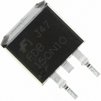
FDB150N10 Fairchild Semiconductor, FDB150N10 Datasheet - Page 6

FDB150N10
Manufacturer Part Number
FDB150N10
Description
MOSFET N-CH 100V 57A D2PAK
Manufacturer
Fairchild Semiconductor
Series
PowerTrench®r
Datasheet
1.FDB150N10.pdf
(8 pages)
Specifications of FDB150N10
Fet Type
MOSFET N-Channel, Metal Oxide
Fet Feature
Standard
Rds On (max) @ Id, Vgs
15 mOhm @ 49A, 10V
Drain To Source Voltage (vdss)
100V
Current - Continuous Drain (id) @ 25° C
57A
Vgs(th) (max) @ Id
4.5V @ 250µA
Gate Charge (qg) @ Vgs
69nC @ 10V
Input Capacitance (ciss) @ Vds
4760pF @ 25V
Power - Max
110W
Mounting Type
Surface Mount
Package / Case
D²Pak, TO-263 (2 leads + tab)
Configuration
Single
Transistor Polarity
N-Channel
Resistance Drain-source Rds (on)
0.015 Ohm @ 10 V
Drain-source Breakdown Voltage
100 V
Gate-source Breakdown Voltage
+/- 20 V
Continuous Drain Current
57 A
Power Dissipation
110000 mW
Maximum Operating Temperature
+ 150 C
Mounting Style
SMD/SMT
Minimum Operating Temperature
- 55 C
Lead Free Status / RoHS Status
Lead free / RoHS Compliant
Other names
FDB150N10TR
FDB150N10 Rev. A
( Driver )
( Driver )
( DUT )
( DUT )
( DUT )
( DUT )
V
V
I
I
V
V
SD
SD
GS
GS
DS
DS
V
V
GS
GS
Peak Diode Recovery dv/dt Test Circuit & Waveforms
R
R
G
G
Driver
Driver
DUT
DUT
I
I
FM
FM
I
I
D =
D =
D =
SD
SD
, Body Diode Forward Current
, Body Diode Forward Current
Forward Voltage Drop
Forward Voltage Drop
--------------------------
--------------------------
--------------------------
Gate Pulse Width
Gate Pulse Width
Gate Pulse Width
Gate Pulse Period
Gate Pulse Period
Gate Pulse Period
Body Diode
Body Diode
Same Type
Same Type
V
V
Body Diode Recovery dv/dt
Body Diode Recovery dv/dt
as DUT
as DUT
+
+
_
_
DS
DS
• dv/dt controlled by R
• dv/dt controlled by R
• I
• I
V
V
SD
SD
SD
SD
Body Diode Reverse Current
Body Diode Reverse Current
controlled by pulse period
controlled by pulse period
6
I
I
RM
RM
L
L L
G
G
di/dt
di/dt
V
V
V
V
10V
10V
DD
DD
DD
DD
www.fairchildsemi.com


