FDMA520PZ Fairchild Semiconductor, FDMA520PZ Datasheet

MOSFET P-CH 20V 7.3A MLP2X2

FDMA520PZ

Manufacturer Part Number
FDMA520PZ
Description
MOSFET P-CH 20V 7.3A MLP2X2
Manufacturer
Fairchild Semiconductor
Series
PowerTrench®r
Datasheet

Specifications of FDMA520PZ

Fet Type
MOSFET P-Channel, Metal Oxide
Fet Feature
Logic Level Gate
Rds On (max) @ Id, Vgs
30 mOhm @ 7.3A, 4.5V
Drain To Source Voltage (vdss)
20V
Current - Continuous Drain (id) @ 25° C
7.3A
Vgs(th) (max) @ Id
1.5V @ 250µA
Gate Charge (qg) @ Vgs
20nC @ 4.5V
Input Capacitance (ciss) @ Vds
1645pF @ 10V
Power - Max
900mW
Mounting Type
Surface Mount
Package / Case
6-MLP, 6-MicroFET™
Transistor Polarity
P Channel
Continuous Drain Current Id
7.3A
Drain Source Voltage Vds
20V
On Resistance Rds(on)
30mohm
Rds(on) Test Voltage Vgs
12V
Threshold Voltage Vgs Typ
-1.1V
Rohs Compliant
Yes
Configuration
Single Quad Drain
Resistance Drain-source Rds (on)
30 mOhms
Forward Transconductance Gfs (max / Min)
22 S
Drain-source Breakdown Voltage
- 20 V
Gate-source Breakdown Voltage
+/- 12 V
Continuous Drain Current
7.3 A
Power Dissipation
2.4 W
Maximum Operating Temperature
+ 150 C
Mounting Style
SMD/SMT
Minimum Operating Temperature
- 55 C
Lead Free Status / RoHS Status
Lead free / RoHS Compliant
Other names
FDMA520PZTR

Available stocks

Company
Part Number
Manufacturer
Quantity
Price
Part Number:
FDMA520PZ
Manufacturer:
FSC
Quantity:
12 400
Part Number:
FDMA520PZ
Manufacturer:
ST
0
Part Number:
FDMA520PZ
Manufacturer:
FAIRCHILD/仙童
Quantity:
20 000
©2009 Fairchild Semiconductor Corporation
FDMA520PZ Rev.B2
MOSFET Maximum Ratings
Thermal Characteristics
Package Marking and Ordering Information
FDMA520PZ
Single P-Channel PowerTrench
–20V, –7.3A, 30m
Features
V
V
I
P
T
R
R
D
J
DS
GS
D
Max r
Max r
Low profile - 0.8mm maximum - in the new package MicroFET
2X2 mm
Free from halogenated compounds and antimony oxides
RoHS Compliant
HBM ESD protection level > 3k V typical (Note 3)
, T
JA
JA
Symbol
Device Marking
STG
DS(on)
DS(on)
520
Drain
= 30m at V
= 53m at V
Pin 1
Drain to Source Voltage
Gate to Source Voltage
Drain Current
Power Dissipation
Power Dissipation
Operating and Storage Junction Temperature Range
Thermal Resistance, Junction to Ambient
MicroFET 2X2 (Bottom View)
D
GS
GS
= –4.5V, I
= –2.5V, I
D
D
FDMA520PZ
-Continuous
-Pulsed
Device
D
S
D
D
= –7.3A
= –5.5A
G
T
A
= 25°C unless otherwise noted
Parameter
Source
MicroFET 2X2
Package
®
MOSFET
1
General Description
This device is designed specifically for battery charge or load
switching in cellular handset and other ultraportable applications.
It features a MOSFET with low on-state resistance.
The MicroFET 2X2 package offers exceptional thermal
performance for its physical size and is well suited to linear mode
applications.
G
D
D
Reel Size
1
2
3
7’’
Bottom Drain Contact
(Note 1a)
(Note 1a)
(Note 1b)
(Note 1a)
(Note 1b)
Tape Width
8mm
–55 to +150
Ratings
–7.3
–20
±12
145
–24
2.4
0.9
52
6
5
4
April 2009
D
D
www.fairchildsemi.com
S
3000 units
Quantity
Units
°C/W
°C
W
V
V
A
tm

Related parts for FDMA520PZ

FDMA520PZ Summary of contents

Page 1

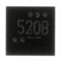
... Thermal Resistance, Junction to Ambient JA Package Marking and Ordering Information Device Marking Device 520 FDMA520PZ ©2009 Fairchild Semiconductor Corporation FDMA520PZ Rev.B2 ® MOSFET General Description = –7.3A This device is designed specifically for battery charge or load D switching in cellular handset and other ultraportable applications. = –5. features a MOSFET with low on-state resistance ...

Page 2

... JA a. 52°C/W when mounted Pulse Test: Pulse Width < 300 s, Duty cycle < 2.0%. 3: The diode connected between the gate and the source serves only as protection against ESD. No gate overvoltage rating is implied. FDMA520PZ Rev. 25°C unless otherwise noted J Test Conditions I = – ...

Page 3

... T , JUNCTION TEMPERATURE J Figure 3. Normalized On- Resistance vs Junction Temperature 24 PULSE DURATION = 80 s DUTY CYCLE = 0.5%MAX - 125 GATE TO SOURCE VOLTAGE (V) GS Figure 5. Transfer Characteristics FDMA520PZ Rev. 25°C unless otherwise noted J PULSE DURATION = 80 s DUTY CYCLE = 0.5%MAX V = -2. 100 125 150 ( 0.001 0.0001 ...

Page 4

... GS 1E 125 C J 1E-6 1E 1E-8 1E GATE TO SOURCE VOLTAGE(V) GS Figure 9. Gate Leakage Current vs Gate to Source Voltage 150 120 PULSE WIDTH (s) Figure 11. Single Pulse Maximum Power Dissipation FDMA520PZ Rev. 25°C unless otherwise noted J 3000 V = -5V DD 1000 V = -10V -15V SINGLE PULSE 145 C = 0.005 ...

Page 5

... Dimensional Outline and Pad Layout FDMA520PZ Rev.B2 5 www.fairchildsemi.com ...

Page 6

... Definition of Terms Datasheet Identification Product Status Advance Information Formative / In Design Preliminary First Production No Identification Needed Full Production Obsolete Not In Production FDMA520PZ Rev. B2 F-PFS™ PowerTrench ® FRFET PowerXS™ SM Global Power Resource Programmable Active Droop™ ® Green FPS™ QFET Green FPS™ ...

Related keywords