PCA9620H/Q900/1,51 NXP Semiconductors, PCA9620H/Q900/1,51 Datasheet - Page 70
PCA9620H/Q900/1,51
Manufacturer Part Number
PCA9620H/Q900/1,51
Description
LCD Drivers 480 SEGMENT LCD SEGMENT DRIVER
Manufacturer
NXP Semiconductors
Datasheet
1.PCA9620HQ900151.pdf
(71 pages)
Specifications of PCA9620H/Q900/1,51
Number Of Segments
60
Maximum Clock Frequency
14500 Hz
Operating Supply Voltage
2.5 V to 5.5 V
Maximum Power Dissipation
400 mW
Maximum Operating Temperature
+ 105 C
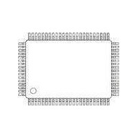
Package / Case
LQFP-80
Maximum Supply Current
200 uA
Minimum Operating Temperature
- 40 C
Lead Free Status / RoHS Status
Lead free / RoHS Compliant
Other names
935291899518
Available stocks
Company
Part Number
Manufacturer
Quantity
Price
Company:

Part Number:
PCA9620H/Q900/1,51
Manufacturer:
NXP Semiconductors
Quantity:
10 000


NXP Semiconductors
20. Contents
1
2
3
4
5
6
6.1
6.2
7
7.1
7.1.1
7.1.2
7.1.3
7.1.4
7.1.5
7.1.6
7.1.7
7.1.8
7.1.9
7.1.10
7.1.11
7.1.12
7.1.12.1
7.1.12.2
7.1.13
7.1.14
7.1.15
7.1.16
7.2
7.3
7.3.1
7.3.2
7.3.3
7.4
7.4.1
7.4.1.1
7.4.2
7.4.2.1
7.4.2.2
7.4.2.3
7.4.2.4
7.4.2.5
7.4.3
7.4.4
7.4.5
7.4.6
PCA9620
Product data sheet
General description . . . . . . . . . . . . . . . . . . . . . . 1
Features and benefits . . . . . . . . . . . . . . . . . . . . 1
Ordering information . . . . . . . . . . . . . . . . . . . . . 2
Marking . . . . . . . . . . . . . . . . . . . . . . . . . . . . . . . . 2
Block diagram . . . . . . . . . . . . . . . . . . . . . . . . . . 2
Pinning information . . . . . . . . . . . . . . . . . . . . . . 3
Functional description . . . . . . . . . . . . . . . . . . . 5
Command: charge-pump-ctrl . . . . . . . . . . . . . . 7
Command: set-VPR-MSB and set-VPR-LSB . . 7
Command: load-data-pointer . . . . . . . . . . . . . . 8
Command: frame-frequency . . . . . . . . . . . . . . . 9
Command: invmode_CPF_ctrl . . . . . . . . . . . . 11
Possible display configurations . . . . . . . . . . . 12
Recommended start-up sequences . . . . . . . . 16
Recommended power-down sequences . . . . 18
V
External V
Charge pump driving capability . . . . . . . . . . . 33
Charge pump frequency settings and power
efficiency. . . . . . . . . . . . . . . . . . . . . . . . . . . . . 33
Pinning . . . . . . . . . . . . . . . . . . . . . . . . . . . . . . . 3
Pin description . . . . . . . . . . . . . . . . . . . . . . . . . 4
Commands of PCA9620 . . . . . . . . . . . . . . . . . . 5
Command: initialize . . . . . . . . . . . . . . . . . . . . . 5
Command: OTP-refresh . . . . . . . . . . . . . . . . . . 6
Command: oscillator-ctrl . . . . . . . . . . . . . . . . . . 6
Command: temp-msr-ctrl . . . . . . . . . . . . . . . . . 7
Command: display-enable . . . . . . . . . . . . . . . . 8
Command: set-MUX-mode . . . . . . . . . . . . . . . . 8
Command: set-bias-mode . . . . . . . . . . . . . . . . 8
Bank select commands . . . . . . . . . . . . . . . . . 10
Command: input-bank-select . . . . . . . . . . . . . 10
Command: output-bank-select . . . . . . . . . . . . 10
Command: write-RAM-data . . . . . . . . . . . . . . 11
Command: temp-read. . . . . . . . . . . . . . . . . . . 11
Command: temp-filter . . . . . . . . . . . . . . . . . . . 12
Start-up and shut-down. . . . . . . . . . . . . . . . . . 14
Power-On Reset (POR) . . . . . . . . . . . . . . . . . 14
LCD voltage . . . . . . . . . . . . . . . . . . . . . . . . . . 20
LCD voltage selector . . . . . . . . . . . . . . . . . . . 20
Electro-optical performance . . . . . . . . . . . . . . 22
LCD drive mode waveforms . . . . . . . . . . . . . . 23
Static drive mode . . . . . . . . . . . . . . . . . . . . . . 23
1:2 Multiplex drive mode. . . . . . . . . . . . . . . . . 24
1:4 Multiplex drive mode. . . . . . . . . . . . . . . . . 26
1:6 Multiplex drive mode. . . . . . . . . . . . . . . . . 27
1:8 Multiplex drive mode. . . . . . . . . . . . . . . . . 29
LCD
generation . . . . . . . . . . . . . . . . . . . . . . . 31
LCD
supply . . . . . . . . . . . . . . . . . . . 32
All information provided in this document is subject to legal disclaimers.
Rev. 1 — 9 December 2010
7.4.7
7.4.8
7.5
7.5.1
7.5.2
7.5.3
7.6
7.7
7.8
7.9
7.9.1
7.9.1.1
7.9.1.2
7.9.1.3
7.9.1.4
7.9.1.5
7.9.2
7.9.2.1
7.9.2.2
8
8.1
8.2
8.3
8.4
8.5
8.6
8.7
8.8
9
10
11
12
13
14
14.1
14.2
14.3
14.4
15
16
17
18
18.1
18.2
18.3
18.4
Universal LCD driver for low multiplex rates
I
Internal circuitry . . . . . . . . . . . . . . . . . . . . . . . 53
Limiting values . . . . . . . . . . . . . . . . . . . . . . . . 54
Static characteristics . . . . . . . . . . . . . . . . . . . 55
Dynamic characteristics. . . . . . . . . . . . . . . . . 59
Package outline. . . . . . . . . . . . . . . . . . . . . . . . 61
Soldering of SMD packages . . . . . . . . . . . . . . 62
Abbreviations . . . . . . . . . . . . . . . . . . . . . . . . . 65
References. . . . . . . . . . . . . . . . . . . . . . . . . . . . 66
Revision history . . . . . . . . . . . . . . . . . . . . . . . 67
Legal information . . . . . . . . . . . . . . . . . . . . . . 68
2
C-bus interface characteristics . . . . . . . . . . 49
Temperature readout . . . . . . . . . . . . . . . . . . . 35
Temperature compensation of V
Oscillator . . . . . . . . . . . . . . . . . . . . . . . . . . . . 38
Internal oscillator . . . . . . . . . . . . . . . . . . . . . . 38
External clock. . . . . . . . . . . . . . . . . . . . . . . . . 38
Timing and frame frequency . . . . . . . . . . . . . 39
Backplane outputs . . . . . . . . . . . . . . . . . . . . . 39
Segment outputs . . . . . . . . . . . . . . . . . . . . . . 40
Display register . . . . . . . . . . . . . . . . . . . . . . . 40
Display RAM . . . . . . . . . . . . . . . . . . . . . . . . . 40
Data pointer . . . . . . . . . . . . . . . . . . . . . . . . . . 41
RAM filling in static drive mode . . . . . . . . . . . 42
RAM filling in 1:2 multiplex drive mode . . . . . 43
RAM filling in 1:4 multiplex drive mode . . . . . 43
RAM filling in 1:6 multiplex drive mode . . . . . 44
RAM filling in 1:8 multiplex drive mode . . . . . 45
Bank selection . . . . . . . . . . . . . . . . . . . . . . . . 46
Input-bank-select . . . . . . . . . . . . . . . . . . . . . . 47
Output-bank-select. . . . . . . . . . . . . . . . . . . . . 48
Bit transfer . . . . . . . . . . . . . . . . . . . . . . . . . . . 49
START and STOP conditions. . . . . . . . . . . . . 49
System configuration . . . . . . . . . . . . . . . . . . . 49
Acknowledge . . . . . . . . . . . . . . . . . . . . . . . . . 50
I
Input filters . . . . . . . . . . . . . . . . . . . . . . . . . . . 51
I
I
Introduction to soldering. . . . . . . . . . . . . . . . . 62
Wave and reflow soldering. . . . . . . . . . . . . . . 62
Wave soldering . . . . . . . . . . . . . . . . . . . . . . . 62
Reflow soldering . . . . . . . . . . . . . . . . . . . . . . 63
Data sheet status . . . . . . . . . . . . . . . . . . . . . . 68
Definitions . . . . . . . . . . . . . . . . . . . . . . . . . . . 68
Disclaimers . . . . . . . . . . . . . . . . . . . . . . . . . . 68
Trademarks . . . . . . . . . . . . . . . . . . . . . . . . . . 69
2
2
2
C-bus controller . . . . . . . . . . . . . . . . . . . . . . 51
C-bus slave address . . . . . . . . . . . . . . . . . . 51
C-bus protocol . . . . . . . . . . . . . . . . . . . . . . . 51
PCA9620
© NXP B.V. 2010. All rights reserved.
LCD
continued >>
. . . . . . . . 36
70 of 71
Related parts for PCA9620H/Q900/1,51
Image
Part Number
Description
Manufacturer
Datasheet
Request
R

Part Number:
Description:
Universal LCD driver for low multiplex rates
Manufacturer:
NXP [NXP Semiconductors]
Datasheet:

Part Number:
Description:
NXP Semiconductors designed the LPC2420/2460 microcontroller around a 16-bit/32-bitARM7TDMI-S CPU core with real-time debug interfaces that include both JTAG andembedded trace
Manufacturer:
NXP Semiconductors
Datasheet:

Part Number:
Description:
NXP Semiconductors designed the LPC2458 microcontroller around a 16-bit/32-bitARM7TDMI-S CPU core with real-time debug interfaces that include both JTAG andembedded trace
Manufacturer:
NXP Semiconductors
Datasheet:
Part Number:
Description:
NXP Semiconductors designed the LPC2468 microcontroller around a 16-bit/32-bitARM7TDMI-S CPU core with real-time debug interfaces that include both JTAG andembedded trace
Manufacturer:
NXP Semiconductors
Datasheet:
Part Number:
Description:
NXP Semiconductors designed the LPC2470 microcontroller, powered by theARM7TDMI-S core, to be a highly integrated microcontroller for a wide range ofapplications that require advanced communications and high quality graphic displays
Manufacturer:
NXP Semiconductors
Datasheet:
Part Number:
Description:
NXP Semiconductors designed the LPC2478 microcontroller, powered by theARM7TDMI-S core, to be a highly integrated microcontroller for a wide range ofapplications that require advanced communications and high quality graphic displays
Manufacturer:
NXP Semiconductors
Datasheet:
Part Number:
Description:
The Philips Semiconductors XA (eXtended Architecture) family of 16-bit single-chip microcontrollers is powerful enough to easily handle the requirements of high performance embedded applications, yet inexpensive enough to compete in the market for hi
Manufacturer:
NXP Semiconductors
Datasheet:
Part Number:
Description:
The XA-S3 device is a member of Philips Semiconductors? XA(eXtended Architecture) family of high performance 16-bitsingle-chip microcontrollers
Manufacturer:
NXP Semiconductors
Datasheet:

Part Number:
Description:
The NXP BlueStreak LH75401/LH75411 family consists of two low-cost 16/32-bit System-on-Chip (SoC) devices
Manufacturer:
NXP Semiconductors
Datasheet:
Part Number:
Description:
The NXP LPC3130/3131 combine an 180 MHz ARM926EJ-S CPU core, high-speed USB2
Manufacturer:
NXP Semiconductors
Datasheet:
Part Number:
Description:
The NXP LPC3141 combine a 270 MHz ARM926EJ-S CPU core, High-speed USB 2
Manufacturer:
NXP Semiconductors
Part Number:
Description:
The NXP LPC3143 combine a 270 MHz ARM926EJ-S CPU core, High-speed USB 2
Manufacturer:
NXP Semiconductors

Part Number:
Description:
The NXP LPC3152 combines an 180 MHz ARM926EJ-S CPU core, High-speed USB 2
Manufacturer:
NXP Semiconductors