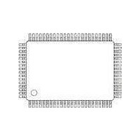
PCA9620H/Q900/1,51 NXP Semiconductors, PCA9620H/Q900/1,51 Datasheet - Page 32

PCA9620H/Q900/1,51
Manufacturer Part Number
PCA9620H/Q900/1,51
Description
LCD Drivers 480 SEGMENT LCD SEGMENT DRIVER
Manufacturer
NXP Semiconductors
Datasheet
1.PCA9620HQ900151.pdf
(71 pages)
Specifications of PCA9620H/Q900/1,51
Number Of Segments
60
Maximum Clock Frequency
14500 Hz
Operating Supply Voltage
2.5 V to 5.5 V
Maximum Power Dissipation
400 mW
Maximum Operating Temperature
+ 105 C
Package / Case
LQFP-80
Maximum Supply Current
200 uA
Minimum Operating Temperature
- 40 C
Lead Free Status / RoHS Status
Lead free / RoHS Compliant
Other names
935291899518
Available stocks
Company
Part Number
Manufacturer
Quantity
Price
Company:
Part Number:
PCA9620H/Q900/1,51
Manufacturer:
NXP Semiconductors
Quantity:
10 000
NXP Semiconductors
PCA9620
Product data sheet
Fig 24. V
V
V
DD2
LCD
(1) If V
(2) Automatic limitation for V
9 V
LCD
00
m
programming of PCA9620 (assuming VT[7:0] = 0h)
7.4.4 External V
DD2
(1)
01
> 3.0 V then VPR[7:0] must be set so that V
n
02
It has to be taken into account that the charge pump has to be configured (via bit CPC)
properly to obtain the desired voltage range. For example, if V
to 2 × V
is V
Section
configured with CPC set to 3 × V
Programmable range of VPR[7:0] is from 0h to FFh. This would allow to achieve
V
In case that V
such that the resultant V
than V
V
not be enabled otherwise a high current may occur on pin V
is supplied externally, no internal temperature compensation occurs on this voltage even if
bit TCE is set logic 1 (see
externally will be available at the segments and backplanes of the device through the
chosen bias system. Also programming the VPR[7:0] bit field has no effect on the V
which is externally supplied.
LCD
LCD
03
LCD
> 9.0 V, but the PCA9620 has a built-in automatic limitation of V
can be directly supplied to the V
04
DD2
= 6.0 V. But in reality, lower values will be reached due to internal resistances, see
DD2
7.4.5. So, if the requested value for V
LCD
.
05
(logic 0) then the maximum theoretical value that the charge pump can reach
LCD
> 9.0 V.
DD2
06
All information provided in this document is subject to legal disclaimers.
supply
is higher than 3.0 V, then it is important that VPR[7:0] is set to a value
. . . . . . . . . . . . . . . . . . . . . . . .
Rev. 1 — 9 December 2010
LCD
Section 7.4.8 on page
(including the temperature correction of VT[7:0]) is higher
LCD
DD2
> V
DD2
(logic 1).
LCD
.
C7
pin. In this case the internal charge pump must
Universal LCD driver for low multiplex rates
C8
(2)
LCD
C9 CA
36). The V
= 7.0 V then the charge pump has to be
. . .
DD2
FC
LCD
DD2
and pin V
FD
voltage which is supplied
= 3.0 V and CPC is set
FE
LCD
PCA9620
© NXP B.V. 2010. All rights reserved.
FF
LCD
at 9.0 V.
VPR[7:0]
013aaa258
. When V
32 of 71
LCD
LCD


