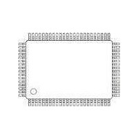
PCA9620H/Q900/1,51 NXP Semiconductors, PCA9620H/Q900/1,51 Datasheet - Page 50

PCA9620H/Q900/1,51
Manufacturer Part Number
PCA9620H/Q900/1,51
Description
LCD Drivers 480 SEGMENT LCD SEGMENT DRIVER
Manufacturer
NXP Semiconductors
Datasheet
1.PCA9620HQ900151.pdf
(71 pages)
Specifications of PCA9620H/Q900/1,51
Number Of Segments
60
Maximum Clock Frequency
14500 Hz
Operating Supply Voltage
2.5 V to 5.5 V
Maximum Power Dissipation
400 mW
Maximum Operating Temperature
+ 105 C
Package / Case
LQFP-80
Maximum Supply Current
200 uA
Minimum Operating Temperature
- 40 C
Lead Free Status / RoHS Status
Lead free / RoHS Compliant
Other names
935291899518
Available stocks
Company
Part Number
Manufacturer
Quantity
Price
Company:
Part Number:
PCA9620H/Q900/1,51
Manufacturer:
NXP Semiconductors
Quantity:
10 000
NXP Semiconductors
PCA9620
Product data sheet
8.4 Acknowledge
The number of data bytes transferred between the START and STOP conditions from
transmitter to receiver is unlimited. Each byte of eight bits is followed by an acknowledge
cycle.
Acknowledgement on the I
Fig 45. System configuration
Fig 46. Acknowledgement on the I
•
•
•
•
A slave receiver which is addressed must generate an acknowledge after the
reception of each byte.
Also a master receiver must generate an acknowledge after the reception of each
byte that has been clocked out of the slave transmitter.
The device that acknowledges must pull-down the SDA line during the acknowledge
clock pulse, so that the SDA line is stable LOW during the HIGH period of the
acknowledge related clock pulse (set-up and hold times must be taken into
consideration).
A master receiver must signal an end of data to the transmitter by not generating an
acknowledge on the last byte that has been clocked out of the slave. In this event the
transmitter must leave the data line HIGH to enable the master to generate a STOP
condition.
SCL
SDA
by transmitter
data output
data output
by receiver
TRANSMITTER/
SCL from
RECEIVER
master
MASTER
All information provided in this document is subject to legal disclaimers.
condition
START
Rev. 1 — 9 December 2010
S
RECEIVER
2
C-bus is shown in
SLAVE
1
2
C-bus
TRANSMITTER/
RECEIVER
Universal LCD driver for low multiplex rates
SLAVE
Figure
2
46.
TRANSMITTER
MASTER
not acknowledge
acknowledge
8
acknowledgement
clock pulse for
PCA9620
TRANSMITTER/
© NXP B.V. 2010. All rights reserved.
RECEIVER
MASTER
9
mbc602
mga807
50 of 71


