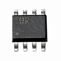
IRF7402TRPBF International Rectifier, IRF7402TRPBF Datasheet - Page 2

IRF7402TRPBF
Manufacturer Part Number
IRF7402TRPBF
Description
MOSFET N-CH 20V 6.8A 8-SOIC
Manufacturer
International Rectifier
Series
HEXFET®r
Datasheet
1.IRF7402TRPBF.pdf
(8 pages)
Specifications of IRF7402TRPBF
Fet Type
MOSFET N-Channel, Metal Oxide
Fet Feature
Logic Level Gate
Rds On (max) @ Id, Vgs
35 mOhm @ 4.1A, 4.5V
Drain To Source Voltage (vdss)
20V
Current - Continuous Drain (id) @ 25° C
6.8A
Vgs(th) (max) @ Id
700mV @ 250µA
Gate Charge (qg) @ Vgs
22nC @ 4.5V
Input Capacitance (ciss) @ Vds
650pF @ 15V
Power - Max
2.5W
Mounting Type
Surface Mount
Package / Case
8-SOIC (3.9mm Width)
Transistor Polarity
N-Channel
Resistance Drain-source Rds (on)
35 mOhms
Drain-source Breakdown Voltage
20 V
Gate-source Breakdown Voltage
12 V
Continuous Drain Current
6.8 A
Power Dissipation
2.5 W
Mounting Style
SMD/SMT
Gate Charge Qg
14 nC
Lead Free Status / RoHS Status
Lead free / RoHS Compliant
Other names
IRF7402PBFTR
IRF7402TRPBF
IRF7402TRPBFTR
IRF7402TRPBF
IRF7402TRPBFTR
Available stocks
Company
Part Number
Manufacturer
Quantity
Price
Part Number:
IRF7402TRPBF
Manufacturer:
IR
Quantity:
20 000
IRF7402PbF
Electrical Characteristics @ T
Notes:
Source-Drain Ratings and Characteristics
V
∆V
V
g
Q
Q
Q
t
t
t
t
C
C
C
I
I
V
t
Q
R
I
d(on)
d(off)
f
I
r
S
SM
DSS
rr
fs
GSS
(BR)DSS
GS(th)
iss
oss
rss
SD
g
gs
gd
DS(on)
Repetitive rating; pulse width limited by
rr
I
T
(BR)DSS
2
max. junction temperature. (See fig. 11)
SD
J
≤ 150°C
≤ 3.8A, di/dt ≤ 96A/µs, V
/∆T
J
Drain-to-Source Breakdown Voltage
Breakdown Voltage Temp. Coefficient
Gate Threshold Voltage
Forward Transconductance
Gate-to-Source Forward Leakage
Gate-to-Source Reverse Leakage
Total Gate Charge
Gate-to-Source Charge
Gate-to-Drain ("Miller") Charge
Turn-On Delay Time
Rise Time
Turn-Off Delay Time
Fall Time
Input Capacitance
Output Capacitance
Reverse Transfer Capacitance
Continuous Source Current
(Body Diode)
Pulsed Source Current
(Body Diode)
Diode Forward Voltage
Reverse Recovery Time
Reverse Recovery Charge
Static Drain-to-Source On-Resistance
Drain-to-Source Leakage Current
Parameter
Parameter
DD
≤ V
(BR)DSS
J
,
= 25°C (unless otherwise specified)
Min. Typ. Max. Units
0.70 –––
Min. Typ. Max. Units
–––
––– 0.024 –––
–––
–––
–––
–––
–––
–––
–––
–––
–––
–––
–––
–––
–––
–––
–––
–––
–––
–––
–––
–––
6.1
20
When mounted on 1 inch square copper board, t<10 sec
Pulse width ≤ 300µs; duty cycle ≤ 2%.
This data sheet has curves & data from IRF7601
150
–––
–––
–––
–––
–––
––– -100
650
300
–––
–––
2.0
6.3
5.1
–––
14
47
24
32
69
51
0.035
0.050
–––
–––
–––
–––
–––
–––
–––
100
–––
–––
–––
100
1.0
3.0
9.5
1.2
25
22
2.5
77
54
V/°C
µA
nA
nC
pF
nC
ns
ns
V
V
S
Ω
V
A
V
Reference to 25°C, I
V
V
V
V
V
V
V
I
V
V
V
I
R
R
V
V
ƒ = 1.0MHz, See Fig. 5
V
di/dt = 100A/µs
MOSFET symbol
showing the
integral reverse
p-n junction diode.
T
T
D
D
GS
GS
GS
DS
DS
DS
DS
GS
GS
DS
GS
DD
GS
DS
J
J
G
D
= 3.8A
= 3.8A
= 25°C, I
= 25°C, I
= 6.2Ω
= 2.6Ω
= V
= 10V, I
= 16V, V
= 16V, V
= 12V
= -12V
= 16V
= 0V
= 15V
= 0V, I
= 4.5V, I
= 2.7V, I
= 4.5V, See Fig. 6 and 12
= 10V
GS
Conditions
, I
D
S
F
D
D
= 250µA
D
D
GS
GS
Conditions
= 3.8A, V
= 3.8A
= 250µA
= 1.9A
= 4.1A
= 3.5A
= 0V
= 0V, T
D
www.irf.com
= 1mA
GS
J
= 125°C
= 0V
G
S
D


