FDB8442 Fairchild Semiconductor, FDB8442 Datasheet - Page 2
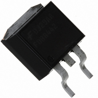
FDB8442
Manufacturer Part Number
FDB8442
Description
MOSFET N-CH 40V 80A D2PAK
Manufacturer
Fairchild Semiconductor
Series
PowerTrench®r
Datasheet
1.FDB8442.pdf
(7 pages)
Specifications of FDB8442
Fet Type
MOSFET N-Channel, Metal Oxide
Fet Feature
Logic Level Gate
Rds On (max) @ Id, Vgs
2.9 mOhm @ 80A, 10V
Drain To Source Voltage (vdss)
40V
Current - Continuous Drain (id) @ 25° C
80A
Vgs(th) (max) @ Id
4V @ 250µA
Gate Charge (qg) @ Vgs
235nC @ 10V
Input Capacitance (ciss) @ Vds
12200pF @ 25V
Power - Max
254W
Mounting Type
Surface Mount
Package / Case
D²Pak, TO-263 (2 leads + tab)
Configuration
Single
Transistor Polarity
N-Channel
Resistance Drain-source Rds (on)
0.005 Ohm @ 10 V
Drain-source Breakdown Voltage
40 V
Gate-source Breakdown Voltage
+/- 20 V
Continuous Drain Current
80 A
Power Dissipation
254000 mW
Maximum Operating Temperature
+ 175 C
Mounting Style
SMD/SMT
Minimum Operating Temperature
- 55 C
Lead Free Status / RoHS Status
Lead free / RoHS Compliant
Other names
FDB8442TR
Available stocks
Company
Part Number
Manufacturer
Quantity
Price
Company:

Part Number:
FDB8442
Manufacturer:
FAIRCHILD
Quantity:
30 000
Company:
Part Number:
FDB8442
Manufacturer:
FAIRCHILD
Quantity:
12 500


FDB8442 Rev. A
MOSFET Maximum Ratings
Thermal Characteristics
Package Marking and Ordering Information
Electrical Characteristics
Off Characteristics
On Characteristics
Dynamic Characteristics
V
V
I
E
P
T
R
R
B
I
I
V
r
C
C
C
R
Q
Q
Q
Q
Q
Symbol
Symbol
D
DSS
GSS
DS(
DSS
GS
AS
D
J
VDSS
GS(th)
θJC
θJA
iss
oss
rss
G
Device Marking
g(TOT)
g(TH)
gs
gs2
gd
, T
on)
STG
FDB8442
Thermal Resistance Junction to Case
Thermal Resistance Junction to Ambient TO-263, lin
Drain to Source Voltage
Gate to Source Voltage
Drain Current Continuous (T
Drain Current Continuous (T
Pulsed
Single Pulse Avalanche Energy
Power Dissipation
Derate above 25
Operating and Storage Temperature
Drain to Source Breakdown Voltage
Zero Gate Voltage Drain Current
Gate to Source Leakage Current
Gate to Source Threshold Voltage
Drain to Source On Resistance
Input Capacitance
Output Capacitance
Reverse Transfer Capacitance
Gate Resistance
Total Gate Charge at 10V
Threshold Gate Charge
Gate to Source Gate Charge
Gate Charge Threshold to Plateau
Gate to Drain “Miller” Charge
FDB8442
Parameter
Device
o
C
C
amb
<158
T
Parameter
J
= 25
TO-263AB
= 25°C unless otherwise noted
Package
T
o
C
C, V
o
= 25°C unless otherwise noted
C, V
GS
GS
V
I
I
T
I
V
V
V
V
f = 1MHz
V
V
V
D
D
D
= 10V)
J
DS
DS
GS
GS
DS
GS
GS
GS
= 10V, with R
= 80A, V
= 80A, V
= 250µA, V
= 175°C
= V
= 32V
= 0V
= 25V, V
= ±20V
= 0.5V, f = 1MHz
= 0 to 10V
= 0 to 2V
Test Conditions
2
GS
2
Reel Size
, I
copper pad area
330mm
GS
GS
D
GS
GS
= 250µA
= 10V
= 10V,
θJA
= 0V,
= 0V
T
V
I
I
D
g
= 43
J
DD
= 1mA
= 80A
= 150°C
= 20V
(Note 1)
o
C/W)
Tape Width
24mm
Min
40
2
-
-
-
-
-
-
-
-
-
-
-
-
-
-
See Figure 4
-55 to +175
Ratings
12200
1040
Typ
2.9
2.1
3.6
640
181
1.0
0.59
±20
23
49
26
41
720
254
1.7
40
80
28
43
-
-
-
-
www.fairchildsemi.com
±100
Max
250
Quantity
800 units
2.9
5.0
235
30
4
1
-
-
-
-
-
-
-
-
Units
Units
W/
o
o
mΩ
C/W
C/W
µA
nC
nC
nC
nC
nC
mJ
nA
pF
pF
pF
o
V
W
Ω
V
V
V
A
C
o
C
Related parts for FDB8442
Image
Part Number
Description
Manufacturer
Datasheet
Request
R

Part Number:
Description:
Fairchild Semiconductor [IGBT MODULE]
Manufacturer:
Fairchild Semiconductor
Datasheet:

Part Number:
Description:
Discrete Semiconductor Modules
Manufacturer:
Fairchild Semiconductor
Part Number:
Description:
Discrete Semiconductor Modules
Manufacturer:
Fairchild Semiconductor
Part Number:
Description:
This N-Channel MOSFET is produced using Fairchild Semiconductor’s advanced Power Trench® process
Manufacturer:
Fairchild Semiconductor
Datasheet:
Part Number:
Description:
This N-Channel MOSFET is produced using Fairchild Semiconductor’s advanced Power Trench® process
Manufacturer:
Fairchild Semiconductor
Datasheet:
Part Number:
Description:
This N-Channel MOSFET is produced using Fairchild Semiconductor’s advanced PowerTrench® process
Manufacturer:
Fairchild Semiconductor
Datasheet:
Part Number:
Description:
This N-Channel MOSFET is produced using Fairchild Semiconductor’s advanced PowerTrench® process
Manufacturer:
Fairchild Semiconductor
Datasheet:
Part Number:
Description:
This N-Channel MOSFET is produced using Fairchild Semiconductor’s advanced Power Trench® process
Manufacturer:
Fairchild Semiconductor
Datasheet:
Part Number:
Description:
This N-Channel logic Level MOSFETs are produced using Fairchild Semiconductor‘s advanced Power Trench® process that has been special tailored to minimize the on-state resistance and yet maintain superior switching performance
Manufacturer:
Fairchild Semiconductor
Datasheet:
Part Number:
Description:
This N-Channel MOSFET is produced using Fairchild Semiconductor’s advanced Power Trench® process
Manufacturer:
Fairchild Semiconductor
Datasheet:
Part Number:
Description:
This N-Channel SyncFET™ is produced using Fairchild Semiconductor’s advanced PowerTrench® process
Manufacturer:
Fairchild Semiconductor
Datasheet:
Part Number:
Description:
This N-Channel SyncFET™ is produced using Fairchild Semiconductor’s advanced PowerTrench® process
Manufacturer:
Fairchild Semiconductor
Datasheet:
Part Number:
Description:
This N-Channel SyncFET™ is produced using Fairchild Semiconductor’s advanced PowerTrench® process
Manufacturer:
Fairchild Semiconductor
Datasheet:
Part Number:
Description:
This N-Channel logic Level MOSFETs are produced using Fairchild Semiconductor‘s advanced Power Trench® process that has been special tailored to minimize the on-state resistance and yet maintain superior switching performance
Manufacturer:
Fairchild Semiconductor
Datasheet:
Part Number:
Description:
This N-Channel MOSFET is produced using Fairchild Semiconductor’s advanced Power Trench® process that has been especially tailored to minimize the on-state resistance and yet maintain superior switching performance
Manufacturer:
Fairchild Semiconductor
Datasheet: