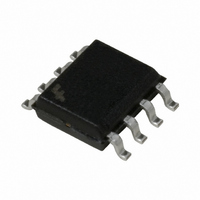
FDS2734 Fairchild Semiconductor, FDS2734 Datasheet - Page 2

FDS2734
Manufacturer Part Number
FDS2734
Description
MOSFET N-CH 250V 3A 8-SOIC
Manufacturer
Fairchild Semiconductor
Series
UltraFET™r
Datasheet
1.FDS2734.pdf
(6 pages)
Specifications of FDS2734
Fet Type
MOSFET N-Channel, Metal Oxide
Fet Feature
Logic Level Gate
Rds On (max) @ Id, Vgs
117 mOhm @ 3A, 10V
Drain To Source Voltage (vdss)
250V
Current - Continuous Drain (id) @ 25° C
3A
Vgs(th) (max) @ Id
4V @ 250µA
Gate Charge (qg) @ Vgs
45nC @ 10V
Input Capacitance (ciss) @ Vds
2610pF @ 100V
Power - Max
1W
Mounting Type
Surface Mount
Package / Case
8-SOIC (3.9mm Width)
Configuration
Single Quad Drain Triple Source
Transistor Polarity
N-Channel
Resistance Drain-source Rds (on)
0.097 Ohms
Forward Transconductance Gfs (max / Min)
15.1 S
Drain-source Breakdown Voltage
250 V
Gate-source Breakdown Voltage
+/- 20 V
Continuous Drain Current
3 A
Power Dissipation
2.5 W
Maximum Operating Temperature
+ 150 C
Mounting Style
SMD/SMT
Minimum Operating Temperature
- 55 C
Lead Free Status / RoHS Status
Lead free / RoHS Compliant
Other names
FDS2734TR
Available stocks
Company
Part Number
Manufacturer
Quantity
Price
Part Number:
FDS2734
Manufacturer:
FSC
Quantity:
20 000
Company:
Part Number:
FDS2734-NL
Manufacturer:
FAIRCHILD
Quantity:
2 500
FDS2734 Rev. B
Electrical Characteristics
Off Characteristics
On Characteristics
Dynamic Characteristics
Switching Characteristics
Drain-Source Diode Characteristics
BV
∆BV
I
I
V
∆V
r
g
C
C
C
R
t
t
t
t
Q
Q
Q
V
t
Q
Notes:
1: R
2: Pulse Test Width <300
3: Starting T
DSS
GSS
d(on)
r
d(off)
f
rr
DS(on)
∆ T
FS
GS(th)
SD
iss
oss
rss
G
g
gs
gd
rr
∆ T
Symbol
drain pins. R
GS(th)
DSS
θJA
DSS
J
J
is the sum of the junction-to-case and case-to-ambient thermal resistance where the case thermal reference is defined as the solder mounting surface of the
J
= 25
θJC
Drain to Source Breakdown Voltage
Breakdown Voltage Temperature
Coefficient
Zero Gate Voltage Drain Current
Gate to Source Leakage Current
Gate to Source Threshold Voltage
Gate to Source Threshold Voltage
Temperature Coefficient
Drain to Source On Resistance
Forward Transconductance
Input Capacitance
Output Capacitance
Reverse Transfer Capacitance
Gate Resistance
Turn-On Delay Time
Rise Time
Turn-Off Delay Time
Fall Time
Total Gate Charge
Gate to Source Gate Charge
Gate to Drain Charge
Source to Drain Diode Voltage
Reverse Recovery Time
Reverse Recovery Charge
°
is guaranteed by design while R
C, L = 1mH, I
µs,
Duty Cycle <2%.
AS
(Note 2)
mounted on a 1in
= 5A, V
a) 50°C/W when
pad of 2 oz copper
Parameter
DD
= 100V, V
θCA
T
is determined by the user’s board design.
J
2
GS
= 25°C unless otherwise noted
= 10V
V
V
V
I
I
V
V
V
V
I
V
V
V
V
V
f = 1MHz
f = 1MHz
I
I
I
D
D
D
SD
F
D
DD
GS
DS
DS
DS
GS
GS
GS
GS
GS
DS
DS
= 3.0 A, d
= 250µA, V
= 250µA, referenced to 25
= 250µA, referenced to 25
= 3.0A
= 3.0A
=10V, I
= 125V, V
= 125V, I
= 200V,V
= 200V, V
= 100V, V
= 10V, R
= ±20V, V
= V
= 10V, I
= 6V , I
= 10V, I
2
DS
Test Conditions
, I
D
D
iF
D
D
D
GS
=3.0A,
D
/dt = 100A/µs
GS
GS
= 2.8A,
GS
GS
= 250µA
= 3.0A,
= 3.0A, T
GS
DS
= 3A
=0 V
= 6Ω
= 0V
= 10V
= 0V T
=0 V
= 0V,
J
J
= 125
= 55
o
o
C
C
o
o
C
C
Scale 1 : 1 on letter size paper
Min
250
b) 125°C/W when
mounted on a minimum
pad of 2 oz copper
2
Typ
-10.7
1960
15.1
157
0.74
101
205
185
0.7
97
23
11
40
11
32
85
26
72
3
9
8
www.fairchildsemi.com
±100
Max
2610
117
126
225
130
278
108
10
1.2
40
37
19
64
19
45
1
4
mV/
Units
mV/
mΩ
nC
µA
nA
pF
pF
pF
nC
nC
nC
ns
ns
ns
ns
ns
V
S
V
Ω
V
o
c
C


