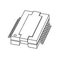
TDF8590TH/N1-T NXP Semiconductors, TDF8590TH/N1-T Datasheet - Page 3

TDF8590TH/N1-T
Manufacturer Part Number
TDF8590TH/N1-T
Description
Audio Amplifiers AMPLIFIER CLASS D
Manufacturer
NXP Semiconductors
Datasheet
1.TDF8590THN1-T.pdf
(30 pages)
Specifications of TDF8590TH/N1-T
Product
Class-D
Output Power
160 W
Available Set Gain
32 dB
Common Mode Rejection Ratio (min)
75 dB
Thd Plus Noise
0.15 %
Maximum Operating Temperature
+ 85 C
Mounting Style
SMD/SMT
Audio Load Resistance
8 Ohms
Dual Supply Voltage
+/- 27 V
Input Signal Type
Differential
Minimum Operating Temperature
- 40 C
Output Signal Type
Differential, Single
Supply Type
Dual
Output Type
1-Channel Mono or 2-Channel Stereo
Package / Case
HSOP-26
Operational Class
Class-D
Audio Amplifier Output Configuration
1-Channel Mono/2-Channel Stereo
Output Power (typ)
160x1@8Ohm/80x2@4OhmW
Audio Amplifier Function
Speaker
Total Harmonic Distortion
0.15@8Ohm@1W%
Single Supply Voltage (typ)
Not RequiredV
Dual Supply Voltage (typ)
±27V
Power Supply Requirement
Dual
Rail/rail I/o Type
No
Single Supply Voltage (min)
Not RequiredV
Single Supply Voltage (max)
Not RequiredV
Dual Supply Voltage (min)
±14V
Dual Supply Voltage (max)
±29V
Operating Temp Range
-40C to 85C
Operating Temperature Classification
Industrial
Mounting
Surface Mount
Pin Count
24
Package Type
HSOP
Lead Free Status / RoHS Status
Lead free / RoHS Compliant
Other names
TDF8590TH/N1,118
NXP Semiconductors
6. Functional description
TDF8590TH_2
Product data sheet
5.2 Pin description
6.1 Introduction
Table 2.
[1]
The TDF8590TH is a dual channel audio power amplifier using class-D technology. The
audio input signal is converted into a Pulse Width Modulated (PWM) signal via an analog
input stage and PWM modulator. To enable the output power transistors to be driven, this
digital PWM signal is applied to a control and handshake block and driver circuits for both
the high-side and low-side. An external 2nd-order low-pass filter converts the PWM output
signal to an analog audio signal across the loudspeakers.
Symbol
V
SGND2
V
IN2M
IN2P
MODE
OSC
IN1P
IN1M
V
SGND1
V
DIAG
V
BOOT1
OUT1
V
STABI
n.c.
V
OUT2
BOOT2
V
V
SSA2
DDA2
DDA1
SSA1
DDP1
SSP1
SSP2
DDP2
SSD
The heatsink is internally connected to pin V
Pin description
Pin
1
2
3
4
5
6
7
8
9
10
11
12
13
14
15
16
17
18
19
20
21
22
23
24
Rev. 02 — 23 April 2007
2
Description
negative analog supply voltage for channel 2
signal ground for channel 2
positive analog supply voltage for channel 2
negative audio input for channel 2
positive audio input for channel 2
mode selection input: standby, mute or operating
oscillator frequency adjustment or tracking input
positive audio input for channel 1
negative audio input for channel 1
positive analog supply voltage for channel 1
signal ground for channel 1
negative analog supply voltage for channel 1
diagnostic for activated current protection
positive power supply voltage for channel 1
bootstrap capacitor for channel 1
PWM output from channel 1
negative power supply voltage for channel 1
decoupling of internal stabilizer for logic supply
not connected
negative power supply voltage for channel 2
PWM output from channel 2
bootstrap capacitor for channel 2
positive power supply voltage for channel 2
negative digital supply voltage
80 W SE (4 ) or 1
SSD
.
160 W BTL (8 ) class-D amplifier
[1]
TDF8590TH
© NXP B.V. 2007. All rights reserved.
3 of 30


