TDF8590TH/N1,518 NXP Semiconductors, TDF8590TH/N1,518 Datasheet
TDF8590TH/N1,518
Specifications of TDF8590TH/N1,518


Related parts for TDF8590TH/N1,518


TDF8590TH/N1,518 Summary of contents
Page 1
TDF8590TH 2 Rev. 02 — 23 April 2007 1. General description The TDF8590TH is a high-efficiency class-D audio power amplifier with low power dissipation for application in car audio systems. The typical output power is 2 into 4 . The ...
Page 2
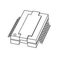
... NXP Semiconductors 4. Block diagram V V DDA2 DDA1 IN1M INPUT 8 STAGE IN1P mute 11 SGND1 7 OSC OSCILLATOR 6 MODE MODE 2 SGND2 mute 5 IN2P INPUT 4 STAGE IN2M SSA2 SSA1 Fig 1. Block diagram 5. Pinning information 5.1 Pinning Fig 2. Pin configuration TDF8590TH_2 Product data sheet STABI ...
Page 3
... NXP Semiconductors 5.2 Pin description Table 2. Symbol V SSA2 SGND2 V DDA2 IN2M IN2P MODE OSC IN1P IN1M V DDA1 SGND1 V SSA1 DIAG V DDP1 BOOT1 OUT1 V SSP1 STABI n.c. V SSP2 OUT2 BOOT2 V DDP2 V SSD [1] The heatsink is internally connected to pin V 6. Functional description 6.1 Introduction The TDF8590TH is a dual channel audio power amplifi ...
Page 4
... NXP Semiconductors The TDF8590TH contains two independent amplifier channels with a differential input stage, high output power, high efficiency (90 %), low distortion and a low quiescent current. The amplifier channels can be connected in the following configurations: • Mono Bridge-Tied Load (BTL) amplifier • ...
Page 5
... NXP Semiconductors The value of the RC time constant should be dimensioned for 500 ms. If the 100 F capacitor is left out of the application the voltage on pin MODE will be applied with a much smaller time constant, which might result in audible pop noises during start-up (depending on DC output offset voltage and used loudspeaker). ...
Page 6
... NXP Semiconductors If two or more class-D amplifiers are used in the same audio application recommended to synchronize the switching frequency of all devices to an external clock (see Section 6.4 Protections The following protections are included in TDF8590TH: • Thermal Foldback (TF) • OverTemperature Protection (OTP) • ...
Page 7
... NXP Semiconductors Fig 5. Pin DIAG with activated current limiting Fig 6. Restart of the TDF8590TH When the loudspeaker terminals are short-circuited and the OCP is triggered the TDF8590TH is switched off completely and will try to restart every 100 ms (see • after switch off pin DIAG will be released • ...
Page 8
... NXP Semiconductors 6.4.4 Window protection The WP checks the conditions at the output terminals of the power stage and is activated: • During the start-up sequence, when pin MODE is switched from standby to mute. In the event of a short-circuit at one of the output terminals to V procedure is interrupted and the TDF8590TH waits until the short to the supply lines has been removed. Because the test is done before enabling the power stages, no large currents will fl ...
Page 9
... NXP Semiconductors [3] Only complete shut down of amplifier in case of a short-circuit. In all other cases current limiting resulting in clipping output signal. [4] Fault condition detected during (every) transition between standby-to-mute and during restart after activation of OCP (short to one of the supply lines). 6.5 Diagnostic output Pin DIAG is pulled LOW when the OCP is triggered ...
Page 10
... NXP Semiconductors a. Internal circuitry b. External connections Fig 8. Input configuration for mono BTL application 7. Limiting values Table 5. Limiting values In accordance with the Absolute Maximum Rating System (IEC 60134). Symbol Parameter V supply voltage DD V negative supply voltage SS V supply voltage P I non-repetitive peak output current ...
Page 11
... NXP Semiconductors Table 5. Limiting values …continued In accordance with the Absolute Maximum Rating System (IEC 60134). Symbol Parameter V voltage on pin MODE MODE V voltage on pin OSC OSC V voltage on pin IN1M IN1M V voltage on pin IN1P IN1P V voltage on pin IN2M IN2M V voltage on pin IN2P IN2P ...
Page 12
... NXP Semiconductors Table 7. Static characteristics 310 kHz + osc amb Symbol Parameter Amplifier outputs; pins OUT1 and OUT2 V output offset voltage O(offset) Stabilizer output; pin STABI (reference output voltage O Temperature protection T protection temperature prot T thermal foldback activation act(th_fold) temperature [1] The circuit is DC adjusted ...
Page 13
... NXP Semiconductors 10. Dynamic characteristics 10.1 Dynamic characteristics (SE) Table 8. Dynamic characteristics (SE kHz otherwise specified. See Section 12 and the capacitor as C. Symbol Parameter P output power o I peak output current OM THD total harmonic distortion P G closed-loop voltage gain v(cl) SVRR supply voltage rejection ...
Page 14
... NXP Semiconductors 10.2 Dynamic characteristics (BTL) Table 9. Dynamic characteristics (BTL kHz otherwise specified. See Section 12 and the capacitor as C. Symbol Parameter P output power o I peak output current OM THD total harmonic distortion P G closed-loop voltage gain v(cl) SVRR supply voltage rejection ...
Page 15
... NXP Semiconductors 11. Switching characteristics Table 10. Switching characteristics + amb Symbol Parameter Internal oscillator f oscillator frequency osc External oscillator or frequency tracking V minimum HIGH-level voltage on pin OSC H(OSC)min V maximum LOW-level voltage on pin OSC L(OSC)max f tracking frequency range track Drain source on-state resistance of the output transistors ...
Page 16
... NXP Semiconductors Peak output current, internally limited SE BTL Variables load resistance L R s(L) R DSon(hs) R DSon(ls oscillator frequency osc t w(min supply voltage [or 0 o(0.5%) I should be below 8 A (see OM and the ripple current. The value of the ripple current is dependent on the coil inductance and voltage drop over the coil. ...
Page 17
... NXP Semiconductors 12.5 Heat sink requirements In some applications it may be necessary to connect an external heat sink to the TDF8590TH. The thermal foldback activates on T the relationship between the maximum power dissipation before activation of the thermal foldback and the total thermal resistance from junction to ambient – ...
Page 18
... NXP Semiconductors The pumping effect should not cause a malfunction of either the audio amplifier and/or the voltage supply source. For instance, this malfunction can be caused by triggering of the UVP, OVP or UBP of the amplifier. Best remedy for pumping effects is to use the TDF8590TH in a mono full-bridge application ...
Page 19
BEAD CON1 470 100 nF ( GND 470 F 100 (35 ...
Page 20
BEAD CON1 470 100 nF ( GND 470 F 100 nF (35 ...
Page 21
... NXP Semiconductors 12.8 Curves measured in reference design 2 10 THD (%) ( kHz. ( kHz. ( 100 Hz Fig 12. Total harmonic distortion as a function of output power, SE application 2 10 THD (%) kHz. ( kHz. ( 100 Hz Fig 13. Total harmonic distortion as a function of output power, BTL application TDF8590TH_2 Product data sheet ...
Page 22
... NXP Semiconductors 1 THD (%) 1 10 ( application Fig 14. Total harmonic distortion as a function of frequency 100 cs (dB) 80 ( Fig 15. Channel separation as a function of frequency TDF8590TH_2 Product data sheet 001aad849 1 THD (%) (kHz ( ( BTL application 001aad851 90 CMRR (dB (kHz) V i(CM) DC shorted. (1) SE application. (2) BTL application. Fig 16. Common mode rejection ratio as a function of frequency Rev. 02 — ...
Page 23
... NXP Semiconductors 120 (1) SVRR (dB) (2) 100 ( (1) ripple on both supply lines, ripple in phase. (2) ripple on both supply lines, ripple in antiphase. (3) ripple on one supply line application Fig 17. Supply voltage ripple rejection as a function of frequency; Standby mode 100 SVRR (dB (1) ( (1) ripple on both supply lines, ripple in phase. ...
Page 24
... NXP Semiconductors 100 SVRR (dB) 80 (1) (2) ( (1) ripple on both supply lines, ripple in phase. (2) ripple on both supply lines, ripple in antiphase. (3) ripple on one supply line application Fig 19. Supply voltage ripple rejection as a function of frequency; Operating mode (RMS). I (1) SE application (2) BTL application Fig 20. Mute attenuation as a function of frequency ...
Page 25
... NXP Semiconductors 120 P o (W) ( kHz. (1) THD = 10 %. (2) THD = 0 Fig 21. Output power as a function of supply voltage, SE application 240 P o (W) (1) 160 ( kHz. (1) THD = 10 %. (2) THD = 0 Fig 22. Output power as a function of supply voltage, BTL application TDF8590TH_2 Product data sheet 001aad860 ( (V) P (1) THD = 10 %. ...
Page 26
... NXP Semiconductors 100 (1) (%) ( kHz application Fig 23. Efficiency as a function of output power 30 P (W) ( kHz application Fig 24. Power dissipation as a function of output power TDF8590TH_2 Product data sheet 001aad865 (%) 60 80 100 P (W) o (1) V (2) V 001aad864 ( 100 P (W) o (1) V (2) V Rev. 02 — 23 April 2007 TDF8590TH 160 W BTL (8 ) class-D amplifi ...
Page 27
... NXP Semiconductors 13. Package outline HSOP24: plastic, heatsink small outline package; 24 leads; low stand-off height pin 1 index DIMENSIONS (mm are the original dimensions) A (1) UNIT max. 0.08 0.53 3.5 mm 3.5 0.35 0.04 0.40 3.2 Notes 1. Limits per individual lead. 2. Plastic or metal protrusions of 0.25 mm maximum per side are not included. ...
Page 28
... Document ID Release date TDF8590TH_2 20070423 • Modifications: The format of this data sheet has been redesigned to comply with the new identity guidelines of NXP Semiconductors. • Legal texts have been adapted to the new company name where appropriate. • All I • Figure 7 • ...
Page 29
... For detailed and full information see the relevant full data sheet, which is available on request via the local NXP Semiconductors sales office. In case of any inconsistency or conflict with the short data sheet, the full data sheet shall prevail ...
Page 30
... NXP Semiconductors 17. Contents 1 General description . . . . . . . . . . . . . . . . . . . . . . 1 2 Features . . . . . . . . . . . . . . . . . . . . . . . . . . . . . . . 1 3 Ordering information . . . . . . . . . . . . . . . . . . . . . 1 4 Block diagram . . . . . . . . . . . . . . . . . . . . . . . . . . 2 5 Pinning information . . . . . . . . . . . . . . . . . . . . . . 2 5.1 Pinning . . . . . . . . . . . . . . . . . . . . . . . . . . . . . . . 2 5.2 Pin description . . . . . . . . . . . . . . . . . . . . . . . . . 3 6 Functional description . . . . . . . . . . . . . . . . . . . 3 6.1 Introduction . . . . . . . . . . . . . . . . . . . . . . . . . . . . 3 6.2 Mode selection . . . . . . . . . . . . . . . . . . . . . . . . . 4 6.3 Pulse width modulation frequency . . . . . . . . . . 5 6.4 Protections . . . . . . . . . . . . . . . . . . . . . . . . . . . . 6 6.4.1 Thermal foldback . . . . . . . . . . . . . . . . . . . . . . . 6 6.4.2 Overtemperature protection . . . . . . . . . . . . . . . 6 6 ...