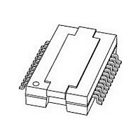
TDF8590TH/N1-T NXP Semiconductors, TDF8590TH/N1-T Datasheet - Page 12

TDF8590TH/N1-T
Manufacturer Part Number
TDF8590TH/N1-T
Description
Audio Amplifiers AMPLIFIER CLASS D
Manufacturer
NXP Semiconductors
Datasheet
1.TDF8590THN1-T.pdf
(30 pages)
Specifications of TDF8590TH/N1-T
Product
Class-D
Output Power
160 W
Available Set Gain
32 dB
Common Mode Rejection Ratio (min)
75 dB
Thd Plus Noise
0.15 %
Maximum Operating Temperature
+ 85 C
Mounting Style
SMD/SMT
Audio Load Resistance
8 Ohms
Dual Supply Voltage
+/- 27 V
Input Signal Type
Differential
Minimum Operating Temperature
- 40 C
Output Signal Type
Differential, Single
Supply Type
Dual
Output Type
1-Channel Mono or 2-Channel Stereo
Package / Case
HSOP-26
Operational Class
Class-D
Audio Amplifier Output Configuration
1-Channel Mono/2-Channel Stereo
Output Power (typ)
160x1@8Ohm/80x2@4OhmW
Audio Amplifier Function
Speaker
Total Harmonic Distortion
0.15@8Ohm@1W%
Single Supply Voltage (typ)
Not RequiredV
Dual Supply Voltage (typ)
±27V
Power Supply Requirement
Dual
Rail/rail I/o Type
No
Single Supply Voltage (min)
Not RequiredV
Single Supply Voltage (max)
Not RequiredV
Dual Supply Voltage (min)
±14V
Dual Supply Voltage (max)
±29V
Operating Temp Range
-40C to 85C
Operating Temperature Classification
Industrial
Mounting
Surface Mount
Pin Count
24
Package Type
HSOP
Lead Free Status / RoHS Status
Lead free / RoHS Compliant
Other names
TDF8590TH/N1,118
NXP Semiconductors
Table 7.
V
[1]
[2]
[3]
[4]
[5]
[6]
TDF8590TH_2
Product data sheet
Symbol
Amplifier outputs; pins OUT1 and OUT2
V
Stabilizer output; pin STABI (reference to V
V
Temperature protection
T
T
P
O(offset)
O
prot
act(th_fold)
= 27 V; f
The circuit is DC adjusted at V
Refers to usage in a symmetrical supply application (see
be defined by an external circuit.
The transition between Standby and Mute mode contains hysteresis, while the slope of the transition between Mute and Operating
mode is determined by the time constant on pin MODE (see
Pin DIAG should not be connected to an external pull-up.
DC output offset voltage is applied to the output during the transition between Mute and Operating mode in a gradual way. The
dV
At a junction temperature of approximately T
approximately T
O(offset)
Static characteristics
/dt caused by any DC output offset is determined by the time constant on pin MODE.
osc
Parameter
output offset voltage
output voltage
protection temperature
thermal foldback activation
temperature
= 310 kHz; T
act(th_fold)
Fig 9. Behavior of pin MODE
+ 5 C the amplifier mutes.
amb
P
= 40 C to +85 C; T
= 12.5 V to 30 V.
…continued
V
O(offset)
operating
mute
act(th_fold)
Conditions
SE; mute
SE; operating
BTL; mute
BTL; operating
mute and operating; with respect
to V
closed loop SE voltage gain
reduced with 6 dB
SSP1
0
SSD
STBY
)
Rev. 02 — 23 April 2007
5 C the gain reduction will commence and at a junction temperature of
j
Section
0.8
= 40 C to +150 C; unless otherwise specified.
2
Figure
80 W SE (4 ) or 1
12.7). In an asymmetrical supply application the SGND voltage should
9).
slope is directly related to the
time constant on pin MODE
2.2
MUTE
2.8
[5]
[5]
[6]
160 W BTL (8 ) class-D amplifier
Min
-
-
-
-
11
-
145
Typ
-
-
-
-
12.5
160
150
4.2
TDF8590TH
V
MODE
ON
© NXP B.V. 2007. All rights reserved.
(V)
001aad842
5.5
Max
20
170
30
240
14
180
-
Unit
mV
mV
mV
mV
V
12 of 30
C
C


