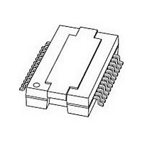
TDF8590TH/N1-T NXP Semiconductors, TDF8590TH/N1-T Datasheet - Page 11

TDF8590TH/N1-T
Manufacturer Part Number
TDF8590TH/N1-T
Description
Audio Amplifiers AMPLIFIER CLASS D
Manufacturer
NXP Semiconductors
Datasheet
1.TDF8590THN1-T.pdf
(30 pages)
Specifications of TDF8590TH/N1-T
Product
Class-D
Output Power
160 W
Available Set Gain
32 dB
Common Mode Rejection Ratio (min)
75 dB
Thd Plus Noise
0.15 %
Maximum Operating Temperature
+ 85 C
Mounting Style
SMD/SMT
Audio Load Resistance
8 Ohms
Dual Supply Voltage
+/- 27 V
Input Signal Type
Differential
Minimum Operating Temperature
- 40 C
Output Signal Type
Differential, Single
Supply Type
Dual
Output Type
1-Channel Mono or 2-Channel Stereo
Package / Case
HSOP-26
Operational Class
Class-D
Audio Amplifier Output Configuration
1-Channel Mono/2-Channel Stereo
Output Power (typ)
160x1@8Ohm/80x2@4OhmW
Audio Amplifier Function
Speaker
Total Harmonic Distortion
0.15@8Ohm@1W%
Single Supply Voltage (typ)
Not RequiredV
Dual Supply Voltage (typ)
±27V
Power Supply Requirement
Dual
Rail/rail I/o Type
No
Single Supply Voltage (min)
Not RequiredV
Single Supply Voltage (max)
Not RequiredV
Dual Supply Voltage (min)
±14V
Dual Supply Voltage (max)
±29V
Operating Temp Range
-40C to 85C
Operating Temperature Classification
Industrial
Mounting
Surface Mount
Pin Count
24
Package Type
HSOP
Lead Free Status / RoHS Status
Lead free / RoHS Compliant
Other names
TDF8590TH/N1,118
NXP Semiconductors
Table 5.
In accordance with the Absolute Maximum Rating System (IEC 60134).
[1]
[2]
[3]
8. Thermal characteristics
9. Static characteristics
Table 7.
V
TDF8590TH_2
Product data sheet
Symbol Parameter
V
V
V
V
V
V
V
V
Symbol
Supply
V
I
I
Mode select input; pin MODE (reference to SGND2)
I
V
Diagnostic output; pin DIAG (reference to V
V
V
Audio inputs; pins IN1M, IN1P (reference to SGND1), IN2P and IN2M (reference to SGND2)
V
q(tot)
stb
MODE
P
MODE
OSC
IN1M
IN1P
IN2M
IN2P
DIAG
O
P
MODE
OL
OH
I
= 27 V; f
Pin BOOT should not be loaded by any other means than the boot capacitor. Shorting pin BOOT to V
Pin STABI should not be loaded by an external circuit. Shorting pin STABI to a voltage source or V
Pin DIAG should not be connected to a voltage source or to a pull-up resistor. An example of a circuit that can be used to read out
diagnostic data is given in
voltage on pin MODE
voltage on pin OSC
voltage on pin IN1M
voltage on pin IN1P
voltage on pin IN2M
voltage on pin IN2P
voltage on pin DIAG
output voltage
Limiting values
Static characteristics
osc
Parameter
supply voltage
total quiescent current
standby current
current on pin MODE
voltage on pin mode
LOW-level output voltage
HIGH-level output voltage
input voltage
= 310 kHz; T
Table 6.
Symbol Parameter
R
R
th(j-c)
th(j-a)
Figure
…continued
amb
= 40 C to +85 C; T
7.
thermal resistance from junction to case
thermal resistance from junction to ambient
Thermal characteristics
Conditions
referred to SGND2
referred to V
referred to SGND1
referred to SGND1
referred to SGND2
referred to SGND2
referred to V
Conditions
no load, no filter, no snubber
network connected
T
V
Standby mode
Mute mode
Operating mode
activated OCP or WP
no activated OCP or WP
j
SSD
MODE
= 40 C to +85 C
)
Rev. 02 — 23 April 2007
= 5.5 V
j
= 40 C to +150 C; unless otherwise specified.
2
SSD
SSD
80 W SE (4 ) or 1
[2][3]
[2][3]
[2][3]
[1]
[4]
[4]
[2]
160 W BTL (8 ) class-D amplifier
Conditions
in free air
[3]
Min
-
-
-
0
2.2
4.2
-
-
-
Min
0
0
0
V
14
5
5
5
5
SSP
SS
will damage the device.
SS
0.3
Typ
50
150
100
-
-
-
-
8.4
0
will damage the device.
TDF8590TH
27
Max
8
40
+5
+5
+5
+5
9
V
© NXP B.V. 2007. All rights reserved.
DDP
Typ
1.1
35
Max
65
500
300
0.8
2.8
6
0.8
9
-
29
+ 0.3 V
Unit
V
V
V
V
V
V
V
Unit
K/W
K/W
Unit
V
mA
V
V
V
V
V
V
11 of 30
A
A


