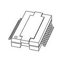
TDF8590TH/N1-T NXP Semiconductors, TDF8590TH/N1-T Datasheet - Page 16

TDF8590TH/N1-T
Manufacturer Part Number
TDF8590TH/N1-T
Description
Audio Amplifiers AMPLIFIER CLASS D
Manufacturer
NXP Semiconductors
Datasheet
1.TDF8590THN1-T.pdf
(30 pages)
Specifications of TDF8590TH/N1-T
Product
Class-D
Output Power
160 W
Available Set Gain
32 dB
Common Mode Rejection Ratio (min)
75 dB
Thd Plus Noise
0.15 %
Maximum Operating Temperature
+ 85 C
Mounting Style
SMD/SMT
Audio Load Resistance
8 Ohms
Dual Supply Voltage
+/- 27 V
Input Signal Type
Differential
Minimum Operating Temperature
- 40 C
Output Signal Type
Differential, Single
Supply Type
Dual
Output Type
1-Channel Mono or 2-Channel Stereo
Package / Case
HSOP-26
Operational Class
Class-D
Audio Amplifier Output Configuration
1-Channel Mono/2-Channel Stereo
Output Power (typ)
160x1@8Ohm/80x2@4OhmW
Audio Amplifier Function
Speaker
Total Harmonic Distortion
0.15@8Ohm@1W%
Single Supply Voltage (typ)
Not RequiredV
Dual Supply Voltage (typ)
±27V
Power Supply Requirement
Dual
Rail/rail I/o Type
No
Single Supply Voltage (min)
Not RequiredV
Single Supply Voltage (max)
Not RequiredV
Dual Supply Voltage (min)
±14V
Dual Supply Voltage (max)
±29V
Operating Temp Range
-40C to 85C
Operating Temperature Classification
Industrial
Mounting
Surface Mount
Pin Count
24
Package Type
HSOP
Lead Free Status / RoHS Status
Lead free / RoHS Compliant
Other names
TDF8590TH/N1,118
NXP Semiconductors
TDF8590TH_2
Product data sheet
12.3 External clock
12.4 Noise
Peak output current, internally limited to 8 A:
SE:
BTL:
Variables:
I
and the ripple current. The value of the ripple current is dependent on the coil inductance
and voltage drop over the coil.
If two or more class-D amplifiers are used it is recommended that all devices run at the
same switching frequency. This can be realized by connecting all OSC pins together and
feed them from an external oscillator.
The internal oscillator requires an external R
V
above SGND. The internal oscillator is disabled and the PWM modulator will switch with
the external frequency. The duty cycle of the external clock should be between 47.5 %
and 52.5 %.
The noise contribution of the internal oscillator is supply voltage dependent. In low noise
applications running at high supply voltage an external low noise oscillator is
recommended.
Noise should be measured using a high-order low-pass filter with a cut-off frequency of
20 kHz. The standard audio band pass filters used in audio analyzers do not suppress the
residue of the carrier frequency sufficiently to ensure a reliable measurement of the
audible noise. Noise measurements should preferably be carried out using AES 17 (Brick
Wall) filters or the Audio Precision AUX 0025 filter, which was designed especially for
measuring switching (class-D) amplifiers.
OM
SSA
R
R
R
R
f
t
V
P
osc
w(min)
P
o(0.5%)
L
s(L)
DSon(hs)
DSon(ls)
should be below 8 A (see
I
. For application of an external oscillator it is necessary to force OSC to a DC level
= load resistance
= supply voltage [or 0.5 (V
OM
I
= oscillator frequency
OM
= series resistance of the filter coil
= minimum pulse width (typical 150 ns, temperature dependent)
=
= output power at the onset of clipping
=
= low side drain source on-state resistance (temperature dependent)
= high side drain source on-state resistance (temperature dependent)
V
----------------------------------------------------------- -
R
-------------------------------------------------------------------------------------------
R
P
L
L
+
+
R
1 t
2V
R
DSon hs
–
DSon hs
P
w min
–
Rev. 02 — 23 April 2007
1 t
+
–
2
+
R
w min
R
Section
f
s L
osc
80 W SE (4 ) or 1
DSon ls
DD
+ V
A
f
SS
7). I
osc
+
)]
2R
OM
ext(OSC)
s L
is the sum of the current through the load
A
and C
160 W BTL (8 ) class-D amplifier
ext(OSC)
TDF8590TH
between pins OSC and
© NXP B.V. 2007. All rights reserved.
16 of 30


