FDG6332C Fairchild Semiconductor, FDG6332C Datasheet
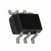
MOSFET N/P-CH 20V SC70-6

FDG6332C

Manufacturer Part Number
FDG6332C
Description
MOSFET N/P-CH 20V SC70-6
Manufacturer
Fairchild Semiconductor
Series
PowerTrench®r
Datasheet

Specifications of FDG6332C

Fet Type
N and P-Channel
Fet Feature
Logic Level Gate
Rds On (max) @ Id, Vgs
300 mOhm @ 700mA, 4.5V
Drain To Source Voltage (vdss)
20V
Current - Continuous Drain (id) @ 25° C
700mA, 600mA
Vgs(th) (max) @ Id
1.5V @ 250µA
Gate Charge (qg) @ Vgs
1.5nC @ 4.5V
Input Capacitance (ciss) @ Vds
113pF @ 10V
Power - Max
300mW
Mounting Type
Surface Mount
Package / Case
SC-70-6, SC-88, SOT-363
Configuration
Dual
Transistor Polarity
N and P-Channel
Resistance Drain-source Rds (on)
0.3 Ohm @ 4.5 V @ N Channel
Forward Transconductance Gfs (max / Min)
2.8 S, 1.8 S
Drain-source Breakdown Voltage
20 V
Gate-source Breakdown Voltage
+/- 12 V
Continuous Drain Current
0.7 A @ N Channel or 0.6 A @ P Channel
Power Dissipation
300 mW
Maximum Operating Temperature
+ 150 C
Mounting Style
SMD/SMT
Minimum Operating Temperature
- 55 C
Module Configuration
Dual
Continuous Drain Current Id
700mA
Drain Source Voltage Vds
20V
On Resistance Rds(on)
300mohm
Rds(on) Test Voltage Vgs
4.5V
Rohs Compliant
Yes
Lead Free Status / RoHS Status
Lead free / RoHS Compliant
Other names
FDG6332C

Available stocks

Company
Part Number
Manufacturer
Quantity
Price
Part Number:
FDG6332C
Manufacturer:
FSC
Quantity:
6 000
Part Number:
FDG6332C
Manufacturer:
FAIRCHILD
Quantity:
5 321
Part Number:
FDG6332C
Manufacturer:
SEMTECH
Quantity:
2 540
Part Number:
FDG6332C
Manufacturer:
FAIRCHILD/仙童
Quantity:
20 000
Company:
Part Number:
FDG6332C
Quantity:
24 962
Company:
Part Number:
FDG6332C
Quantity:
2 500
Company:
Part Number:
FDG6332C
Quantity:
127
Part Number:
FDG6332C-F085
0
Part Number:
FDG6332C-NL
Manufacturer:
NP20V07A
Quantity:
20 000
Part Number:
FDG6332C_F085
Manufacturer:
FAIRCHILD/仙童
Quantity:
20 000
Part Number:
FDG6332C_NL
Manufacturer:
ON/安森美
Quantity:
20 000
2003 Fairchild Semiconductor Corporation
FDG6332C
20V N & P-Channel PowerTrench MOSFETs
General Description
The N & P-Channel MOSFETs are produced using
Fairchild Semiconductor’s advanced PowerTrench
process that has been especially tailored to minimize
on-state resistance and yet maintain superior
switching performance.
These
exceptional power dissipation in a very small footprint
for applications where the bigger more expensive
TSSOP-8 and SSOP-6 packages are impractical.
Applications
Absolute Maximum Ratings
Symbol
V
V
I
P
T
Thermal Characteristics
R
Package Marking and Ordering Information
D
DC/DC converter
Load switch
LCD display inverter
J
DSS
GSS
D
, T
JA
Device Marking
STG
devices
.32
Drain-Source Voltage
Gate-Source Voltage
Drain Current
Power Dissipation for Single Operation
Operating and Storage Junction Temperature Range
Thermal Resistance, Junction-to-Ambient
have
D
Pin 1
G
been
S
SC70-6
– Continuous
– Pulsed
FDG6332C
designed
S
Device
Parameter
G
D
to
offer
T
A
=25
o
C unless otherwise noted
Reel Size
7’’
(Note 1)
(Note 1)
(Note 1)
Features
Q1
Q2
Low gate charge
High performance trench technology for extremely
low R
SC70-6 package: small footprint (51% smaller than
SSOT-6); low profile (1mm thick)
0.7 A, 20V.
–0.6 A, –20V.
DS(ON)
1
2
3
Q1
0.7
2.1
20
12
Tape width
–55 to +150
8mm
Complementary
R
R
R
R
DS(ON)
DS(ON)
DS(ON)
DS(ON)
415
0.3
= 300 m
= 400 m
= 420 m
= 630 m
September 2003
–0.6
Q2
–20
–2
12
6
4
5
@ V
@ V
@ V
@ V
FDG6332C Rev C2 (W)
3000 units
Quantity
GS
GS
GS
GS
= 4.5 V
= 2.5 V
= –4.5 V
= –2.5 V
Units
C/W
W
V
V
A
C

Related parts for FDG6332C

FDG6332C Summary of contents

Page 1

... Reel Size 7’’ September 2003 R = 300 4.5 V DS(ON 400 2.5 V DS(ON 420 –4.5 V DS(ON 630 –2.5 V DS(ON Complementary Q1 Q2 Units 20 – 0.7 –0.6 A 2.1 –2 0.3 W –55 to +150 C C/W 415 Tape width Quantity 8mm 3000 units FDG6332C Rev C2 (W) ...

Page 2

... A –1 100 nA 100 nA 0.6 1.1 1.5 V -0.6 –1.2 –1.5 –2.8 mV 180 300 m 400 293 442 247 300 420 470 630 700 400 2 –2 113 pF 114 5 1 1.7 3.4 1.1 1.5 nC 1.4 2 0.24 nC 0.3 0.3 nC 0.4 FDG6332C Rev C2 (W) ...

Page 3

... Pulse Test: Pulse Width < 300 s, Duty Cycle < 2. 25°C unless otherwise noted A Test Conditions 0. (Note –0. (Note determined by the user's board design 415°C/W when mounted on a minimum pad of FR Min Typ Max Units 0. –0.25 Q2 0.74 1.2 V –0.77 –1.2 FDG6332C Rev C2 (W) ...

Page 4

... Figure 6. Body Diode Forward Voltage Variation with Source Current and Temperature. 3.0V 3.5V 4.0V 4. DRAIN CURRENT ( =0. 125 GATE TO SOURCE VOLTAGE (V) GS Gate-to-Source Voltage 125 -55 C 0.2 0.4 0.6 0 BODY DIODE FORWARD VOLTAGE (V) SD FDG6332C Rev C2 ( 1.2 ...

Page 5

... C RSS 0 0 1.2 1.6 Figure 8. Capacitance Characteristics. 10 100 s 8 1ms 0.001 100 Figure 10. Single Pulse Maximum f = 1MHz ISS C OSS DRAIN TO SOURCE VOLTAGE (V) DS SINGLE PULSE R = 415°C 25°C A 0.01 0 TIME (sec) 1 Power Dissipation. FDG6332C Rev C2 (W) 20 100 ...

Page 6

... Figure 16. Body Diode Forward Voltage Variation with Source Current and Temperature. -3.0V -3.5V -4.0V -4.5V 0 DRAIN CURRENT ( -0 125 GATE TO SOURCE VOLTAGE (V) GS Gate-to-Source Voltage 125 -55 C 0.2 0.4 0.6 0 BODY DIODE FORWARD VOLTAGE (V) SD FDG6332C Rev C2 ( 1.2 ...

Page 7

... Figure 18. Capacitance Characteristics 100 s 1ms 100 0.001 Figure 20. Single Pulse Maximum 0.01 0 TIME (sec 1MHz ISS C OSS DRAIN TO SOURCE VOLTAGE (V) DS SINGLE PULSE 415 C 0.01 0 SINGLE PULSE TIME (SEC) Power Dissipation. R ( 415 °C/W JA P(pk ( Duty Cycle FDG6332C Rev C2 (W) 20 100 100 ...

Page 8

... TRADEMARKS The following are registered and unregistered trademarks Fairchild Semiconductor owns or is authorized to use and is not intended exhaustive list of all such trademarks. ACEx™ FACT Quiet Series™ ActiveArray™ FAST Bottomless™ FASTr™ CoolFET™ FRFET™ CROSSVOLT™ ...

Related keywords