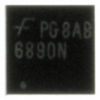
FDMC6890NZ Fairchild Semiconductor, FDMC6890NZ Datasheet

FDMC6890NZ
Specifications of FDMC6890NZ
Related parts for FDMC6890NZ
FDMC6890NZ Summary of contents
Page 1
... Device Marking Device 6890N FDMC6890NZ ©2006 Fairchild Semiconductor Corporation FDMC6890NZ Rev.C ® MOSFET General Description FDMC6890NZ is a compact single package solution for converters = 4A D characteristics. Inside the Power 33 package features two = 3A D N-channel MOSFETs with low on-state resistance and low gate charge to efficiency ...
Page 2
... Turn-Off Delay Time d(off) t Fall Time f Q Total Gate Charge at 4.5V g(TOT) Q Total Gate Charge at 2V g(2) Q Gate to Source Gate Charge gs Q Gate to Drain “Miller” Charge gd FDMC6890NZ Rev 25°C unless otherwise noted J Test Conditions I = 250µ 250µA, referenced to 25° 16V ...
Page 3
... SD t Reverse Recovery Time rr Q Reverse Recovery Charge rr Notes determined with the device mounted on a 1in θJA the user's board design. 2: Pulse Test: Pulse Width < 300µs, Duty cycle < 2.0%. FDMC6890NZ Rev 25°C unless otherwise noted J Test Conditions = 0V 4A, di/dt = 100A pad 2 oz copper pad on a 1.5 x 1.5 in. board of FR-4 material 65° ...
Page 4
... JUNCTION TEMPERATURE J Figure 3. Normalized On - Resistance vs Junction Temperature 9 µ PULSE DURATION = DUTY CYCLE = 0.5%MAX 0.0 0.5 1 GATE TO SOURCE VOLTAGE (V) GS Figure 5. Transfer Characteristics FDMC6890NZ Rev 25°C unless otherwise noted J PULSE DURATION = 80 µ s DUTY CYCLE = 0.5%MAX 2.0 2.5 3.0 75 100 125 150 150 ...
Page 5
... Gate Charge Characteristics 125 0.01 0 TIME IN AVALANCHE(ms) AV Figure 9. Unclamped Inductive Switching Capability 100 V = 10V SINGLE PULSE 0 Figure 11. FDMC6890NZ Rev 25°C unless otherwise noted 10V 12V DD 2.0 2.5 3 0.1 0. PULSE WIDTH (s) Single Pulse Maximum Power Dissipation 5 400 C iss 100 C oss C rss f = 1MHz ...
Page 6
... Typical Characteristics (Q1 N-Channel DUTY CYCLE-DESCENDING ORDER D = 0.5 0.2 0.1 0.05 0.02 0.1 0.01 SINGLE PULSE 0.01 0.006 - FDMC6890NZ Rev 25°C unless otherwise noted RECTANGULAR PULSE DURATION (s) Figure 12. Transient Thermal Response Curve NOTES: DUTY FACTOR PEAK θJA θ www.fairchildsemi.com 3 10 ...
Page 7
... Figure 15. Normalized On Resistance vs Junction Temperature 6 PULSE DURATION = 80 µ DUTY CYCLE = 0.5%MAX 0.0 0.5 1.0 1 GATE TO SOURCE VOLTAGE (V) GS Figure 17. Transfer Characteristics FDMC6890NZ Rev.C PULSE DURATION = 80 µ s DUTY CYCLE = 0.5%MAX 1.8V GS 1.5 2.0 2.5 Figure 14. Normalized on-Resistance vS Drain 75 100 125 150 ...
Page 8
... GATE CHARGE(nC) g Figure 19. Gate Charge Characteristics 125 1E-3 0. TIME IN AVALANCHE(ms) AV Figure 21. Unclamped Inductive Switching Capability 200 100 V = 10V GS 10 SINGLE PULSE FDMC6890NZ Rev 12V DD 1.2 1 PULSE WIDTH (s) Figure 23. Single Pulse Maximum Power Dissipation 8 400 100 f = 1MHz 0 DRAIN TO SOURCE VOLTAGE (V) DS Figure 20 ...
Page 9
... Typical Characteristics 2 1 DUTY CYCLE-DESCENDING ORDER D = 0.5 0.2 0.1 0.05 0.1 0.02 0.01 0.01 SINGLE PULSE 1E FDMC6890NZ Rev RECTANGULAR PULSE DURATION (s) Figure 24. Transient Thermal Response Curve NOTES: DUTY FACTOR PEAK θJA θ www.fairchildsemi.com 3 10 ...
Page 10
... FDMC6890NZ Rev.C 10 www.fairchildsemi.com ...
Page 11
... PRODUCT STATUS DEFINITIONS Definition of Terms Datasheet Identification Advance Information Preliminary No Identification Needed Obsolete FDMC6890NZ Rev. C OCX™ SILENT SWITCHER OCXPro™ SMART START™ ® OPTOLOGIC SPM™ OPTOPLANAR™ Stealth™ ...


