SI4569DY-T1-E3 Vishay, SI4569DY-T1-E3 Datasheet - Page 4
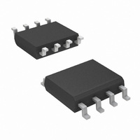
SI4569DY-T1-E3
Manufacturer Part Number
SI4569DY-T1-E3
Description
MOSFET N/P-CH 40V 8-SOIC
Manufacturer
Vishay
Series
TrenchFET®r
Datasheet
1.SI4569DY-T1-E3.pdf
(12 pages)
Specifications of SI4569DY-T1-E3
Transistor Polarity
N and P-Channel
Fet Type
N and P-Channel
Fet Feature
Standard
Rds On (max) @ Id, Vgs
27 mOhm @ 6A, 10V
Drain To Source Voltage (vdss)
40V
Current - Continuous Drain (id) @ 25° C
6A, 6.1A
Vgs(th) (max) @ Id
2V @ 250µA
Gate Charge (qg) @ Vgs
32nC @ 10V
Input Capacitance (ciss) @ Vds
855pF @ 20V
Power - Max
2W
Mounting Type
Surface Mount
Package / Case
8-SOIC (3.9mm Width)
Minimum Operating Temperature
- 55 C
Configuration
Dual Dual Drain
Resistance Drain-source Rds (on)
0.027 Ohm @ 10 V @ N Channel
Drain-source Breakdown Voltage
40 V
Gate-source Breakdown Voltage
+/- 16 V
Continuous Drain Current
6 A @ N Channel or 6.1 A @ P Channel
Power Dissipation
2000 mW
Maximum Operating Temperature
+ 150 C
Mounting Style
SMD/SMT
Module Configuration
Dual
Continuous Drain Current Id
6A
Drain Source Voltage Vds
40V
On Resistance Rds(on)
27mohm
Rds(on) Test Voltage Vgs
10V
Lead Free Status / RoHS Status
Lead free / RoHS Compliant
Lead Free Status / RoHS Status
Lead free / RoHS Compliant, Lead free / RoHS Compliant
Other names
SI4569DY-T1-E3TR
Available stocks
Company
Part Number
Manufacturer
Quantity
Price

Part Number:
SI4569DY-T1-E3
Manufacturer:
VISHAY/威世
Quantity:
20 000


Si4569DY
Vishay Siliconix
N-CHANNEL TYPICAL CHARACTERISTICS 25 °C, unless otherwise noted
www.vishay.com
4
0.030
0.028
0.026
0.024
0.022
0.020
0.018
10
20
16
12
8
6
4
2
0
On-Resistance vs. Drain Current and Gate Voltage
8
4
0
0.0
0.0
0
I
D
= 5 A
V
GS
4.4
0.5
V
4
= 4.5 V
V
DS
Q
DS
Output Characteristics
g
- Drain-to-Source Voltage (V)
= 20 V
- Total Gate Charge (nC)
I
D
V
V
GS
GS
- Drain Current (A)
Gate Charge
8.8
1.0
8
= 10 V
= 10 thru 3 V
V
DS
= 10 V
13.2
1.5
12
V
DS
= 30 V
2 V
17.6
2.0
16
22.0
2.5
20
1400
1120
840
560
280
2.0
1.7
1.4
1.1
0.8
0.5
2.0
1.6
1.2
0.8
0.4
0.0
0
- 50
0.0
0
On-Resistance vs. Junction Temperature
I
D
- 25
= 5 A
0.5
V
V
8
DS
T
GS
J
T
Transfer Characteristics
0
- Junction Temperature (°C)
C
- Drain-to-Source Voltage (V)
- Gate-to-Source Voltage (V)
= 125 °C
C
1.0
rss
25
25 °C
Capacitance
16
S09-0393-Rev. B, 09-Mar-09
50
1.5
C
V
iss
GS
Document Number: 73586
C
oss
= 4.5 V
24
75
2.0
V
- 55 °C
GS
100
= 10 V
32
2.5
125
150
3.0
40
Related parts for SI4569DY-T1-E3
Image
Part Number
Description
Manufacturer
Datasheet
Request
R

Part Number:
Description:
N- And P-channel 40-v D-s Mosfet
Manufacturer:
Vishay
Datasheet:
Part Number:
Description:
357-036-542-201 CARDEDGE 36POS DL .156 BLK LOPRO
Manufacturer:
Vishay
Datasheet:
Part Number:
Description:
357-036-542-201 CARDEDGE 36POS DL .156 BLK LOPRO
Manufacturer:
Vishay
Datasheet:
Part Number:
Description:
357-036-542-201 CARDEDGE 36POS DL .156 BLK LOPRO
Manufacturer:
Vishay
Datasheet:
Part Number:
Description:
357-036-542-201 CARDEDGE 36POS DL .156 BLK LOPRO
Manufacturer:
Vishay
Datasheet:
Part Number:
Description:
357-036-542-201 CARDEDGE 36POS DL .156 BLK LOPRO
Manufacturer:
Vishay
Datasheet:
Part Number:
Description:
357-036-542-201 CARDEDGE 36POS DL .156 BLK LOPRO
Manufacturer:
Vishay
Datasheet:
Part Number:
Description:
357-036-542-201 CARDEDGE 36POS DL .156 BLK LOPRO
Manufacturer:
Vishay
Datasheet:
Part Number:
Description:
357-036-542-201 CARDEDGE 36POS DL .156 BLK LOPRO
Manufacturer:
Vishay
Datasheet:
Part Number:
Description:
357-036-542-201 CARDEDGE 36POS DL .156 BLK LOPRO
Manufacturer:
Vishay
Datasheet:
Part Number:
Description:
357-036-542-201 CARDEDGE 36POS DL .156 BLK LOPRO
Manufacturer:
Vishay
Datasheet:
Part Number:
Description:
357-036-542-201 CARDEDGE 36POS DL .156 BLK LOPRO
Manufacturer:
Vishay
Datasheet:
Part Number:
Description:
357-036-542-201 CARDEDGE 36POS DL .156 BLK LOPRO
Manufacturer:
Vishay
Datasheet:
Part Number:
Description:
357-036-542-201 CARDEDGE 36POS DL .156 BLK LOPRO
Manufacturer:
Vishay
Datasheet: