FDMS9620S Fairchild Semiconductor, FDMS9620S Datasheet
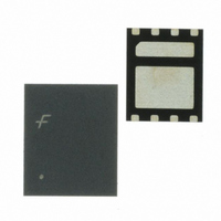
MOSFET N-CHAN DUAL 30V POWER56

FDMS9620S

Manufacturer Part Number
FDMS9620S
Description
MOSFET N-CHAN DUAL 30V POWER56
Manufacturer
Fairchild Semiconductor
Series
PowerTrench®r
Datasheet

Specifications of FDMS9620S

Fet Type
2 N-Channel (Dual)
Fet Feature
Logic Level Gate
Rds On (max) @ Id, Vgs
21.5 mOhm @ 7.5A, 10V
Drain To Source Voltage (vdss)
30V
Current - Continuous Drain (id) @ 25° C
7.5A, 10A
Vgs(th) (max) @ Id
3V @ 250µA
Gate Charge (qg) @ Vgs
14nC @ 10V
Input Capacitance (ciss) @ Vds
665pF @ 15V
Power - Max
1W
Mounting Type
Surface Mount
Package / Case
8-MLP, Power56
Configuration
Dual
Transistor Polarity
N-Channel
Resistance Drain-source Rds (on)
0.0215 Ohm @ 10 V @ Q1
Forward Transconductance Gfs (max / Min)
28 S / 27 S
Drain-source Breakdown Voltage
30 V
Gate-source Breakdown Voltage
+/- 20 V
Continuous Drain Current
7.5 A @ Q1 or 10 A @ Q2
Power Dissipation
2500 mW
Maximum Operating Temperature
+ 150 C
Mounting Style
SMD/SMT
Minimum Operating Temperature
- 55 C
Module Configuration
Dual
Continuous Drain Current Id
10A
Drain Source Voltage Vds
30V
On Resistance Rds(on)
18mohm
Rds(on) Test Voltage Vgs
20V
Rohs Compliant
Yes
Lead Free Status / RoHS Status
Lead free / RoHS Compliant
Other names
FDMS9620STR

Available stocks

Company
Part Number
Manufacturer
Quantity
Price
Part Number:
FDMS9620S
Manufacturer:
FSC
Quantity:
2 001
Part Number:
FDMS9620S
Manufacturer:
FAIRCHILD
Quantity:
2 139
Part Number:
FDMS9620S
Manufacturer:
FAIRCHILD/仙童
Quantity:
20 000
Company:
Part Number:
FDMS9620S
Quantity:
6 000
Company:
Part Number:
FDMS9620S
Quantity:
1 500
Company:
Part Number:
FDMS9620S
Quantity:
4 500
©2007 Fairchild Semiconductor Corporation
FDMS9620S Rev.D3
FDMS9620S
Dual N-Channel PowerTrench
Q1: 30V, 16A, 21.5mΩ Q2: 30V, 18A, 13mΩ
Features
Q1: N-Channel
Q2: N-Channel
MOSFET Maximum Ratings
Thermal Characteristics
Package Marking and Ordering Information
V
V
I
P
T
R
R
R
D
DS
GS
D
J
θJC
θJA
θJA
Max r
Max r
Max r
Max r
Low Qg high side MOSFET
Low r
Thermally efficient dual Power 56 package
Pinout optimized for simple PCB design
RoHS Compliant
, T
Symbol
Device Marking
STG
FDMS9620S
DS(on)
DS(on)
DS(on)
DS(on)
DS(on)
= 21.5mΩ at V
= 29.5mΩ at V
= 13mΩ at V
= 17mΩ at V
low side MOSFET
Drain to Source Voltage
Gate to Source Voltage
Drain Current
Power Dissipation for Single Operation
Operating and Storage Junction Temperature Range
Thermal Resistance, Junction to Case
Thermal Resistance, Junction to Ambient
G2
G2
S2
S2
GS
GS
GS
GS
S2
S2
Power 56
= 10V, I
= 4.5V, I
FDMS9620S
= 10V, I
= 4.5V, I
S2
S2
Device
-Continuous (Package limited) T
-Continuous (Silicon limited)
-Continuous
-Pulsed
S1/D2
S1/D2
D
D
D
= 10A
D
= 8.5A
= 7.5A
= 6.5A
D1
D1
G1
G1
T
A
D1
D1
= 25°C unless otherwise noted
D1
D1
Parameter
D1
D1
®
Power 56
Package
MOSFET
1
T
T
T
T
C
C
A
A
General Description
This device includes two specialized MOSFETs in a unique dual
Power 56 package.
Synchronous Buck power stage in terms of efficiency and PCB
utilization.
complemented by a Low Conduction Loss "Low Side" SyncFET.
Applications
Synchronous Buck Converter for:
A
= 25°C
= 25°C
= 25°C
= 25°C
= 25°C
Notebook System Power
General Purpose Point of Load
S2
S2
S2
G2
Reel Size
The low switching loss "High Side" MOSFET is
13”
5
6
7
8
(Note 1a)
(Note 1a)
(Note 1b)
(Note 1a)
(Note 1b)
Q2
It is designed to provide an optimal
Tape Width
±20
Q1
7.5
8.2
12mm
30
16
21
60
Q1
-55 to +150
120
2.5
50
4
3
2
1
1
D1
D1
D1
G1
August 2007
±20
Q2
3.1
30
18
44
10
60
www.fairchildsemi.com
3000 units
Quantity
Units
°C/W
°C
W
V
V
A
tm

Related parts for FDMS9620S

FDMS9620S Summary of contents

Page 1

... R Thermal Resistance, Junction to Ambient θJA Package Marking and Ordering Information Device Marking Device FDMS9620S FDMS9620S ©2007 Fairchild Semiconductor Corporation FDMS9620S Rev.D3 ® MOSFET General Description = 7.5A D This device includes two specialized MOSFETs in a unique dual = 6.5A D Power 56 package. Synchronous Buck power stage in terms of efficiency and PCB = 10A utilization ...

Page 2

... Turn-Off Delay Time d(off) t Fall Time f Q Total Gate Charge g Q Gate to Source Gate Charge gs Q Gate to Drain “Miller” Charge gd ©2007 Fairchild Semiconductor Corporation FDMS9620S Rev. 25°C unless otherwise noted J Test Conditions I = 250μ 1mA 250μA, referenced to 25°C ...

Page 3

... Reverse Recovery Charge rr Notes determined with the device mounted on a 1in θJA the user's board design. 2: Pulse Test: Pulse Width < 300μs, Duty cycle < 2.0%. ©2007 Fairchild Semiconductor Corporation FDMS9620S Rev. 25°C unless otherwise noted J Test Conditions 2.1A (Note 2) GS ...

Page 4

... Figure 3. Normalized On Resistance vs Junction Temperature 40 μ PULSE DURATION = 300 DUTY CYCLE = 2.0%MAX =125 GATE TO SOURCE VOLTAGE (V) GS Figure 5. Transfer Characteristics ©2007 Fairchild Semiconductor Corporation FDMS9620S Rev. 25°C unless otherwise noted J 2 4.5V 2 1.8 1 3.5V GS 1.4 μ 1.2 s 1.0 ...

Page 5

... V , DRAIN to SOURCE VOLTAGE (V) DS Figure 9. Forward Bias Safe Operating Area 2 1 DUTY CYCLE-DESCENDING ORDER D = 0.5 0.2 0.1 0.05 0.02 0.01 0.1 0. ©2007 Fairchild Semiconductor Corporation FDMS9620S Rev. 25°C unless otherwise noted J =10V V = 15V 20V 100 1ms 10ms 100ms 1s 10s DC 10 100 ...

Page 6

... Junction Temperature 60 PULSE DURATION = 300 DUTY CYCLE = 2.0%MAX =125 GATE TO SOURCE VOLTAGE (V) GS Figure 16. Transfer Characteristics ©2007 Fairchild Semiconductor Corporation FDMS9620S Rev. 4. 3.5V GS μ PULSE DURATION = 300 s DUTY CYCLE = 2.0%MAX 1.5 2.0 2.5 Figure 13. Normalized on-Resistance vs Drain 75 100 125 150 μ ...

Page 7

... Typical Characteristics 10A GATE CHARGE(nC) g Figure 18. Gate Charge Characteristics ©2007 Fairchild Semiconductor Corporation FDMS9620S Rev.D3 =10V 15V 20V 2000 1000 100 f = 1MHz 0 DRAIN TO SOURCE VOLTAGE (V) DS Figure 19. Capacitance vs Drain to Source Voltage C iss C oss C rss 30 10 www.fairchildsemi.com ...

Page 8

... Dimensional Outline and Pad Layout ©2007 Fairchild Semiconductor Corporation FDMS9620S Rev.D3 8 www.fairchildsemi.com ...

Page 9

... Product Status Advance Information Formative or In Design Preliminary First Production No Identification Needed Full Production Obsolete Not In Production ©2007 Fairchild Semiconductor Corporation FDMS9620S Rev.D3 FPS™ PDP-SPM™ F-PFS™ Power-SPM™ ® FRFET PowerTrench SM Global Power Resource Programmable Active Droop™ ...

Related keywords