FDC6333C Fairchild Semiconductor, FDC6333C Datasheet
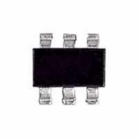
MOSFET N-CH/P-CHAN 30V SSOT6

FDC6333C

Manufacturer Part Number
FDC6333C
Description
MOSFET N-CH/P-CHAN 30V SSOT6
Manufacturer
Fairchild Semiconductor
Series
PowerTrench®r
Datasheet

Specifications of FDC6333C

Fet Type
N and P-Channel
Fet Feature
Logic Level Gate
Rds On (max) @ Id, Vgs
95 mOhm @ 2.5A, 10V
Drain To Source Voltage (vdss)
30V
Current - Continuous Drain (id) @ 25° C
2.5A, 2A
Vgs(th) (max) @ Id
3V @ 250µA
Gate Charge (qg) @ Vgs
6.6nC @ 10V
Input Capacitance (ciss) @ Vds
282pF @ 15V
Power - Max
700mW
Mounting Type
Surface Mount
Package / Case
6-SSOT, SuperSOT-6
Configuration
Dual
Transistor Polarity
N and P-Channel
Resistance Drain-source Rds (on)
0.095 Ohm @ 10 V @ N Channel
Forward Transconductance Gfs (max / Min)
7 S, 3 S
Drain-source Breakdown Voltage
30 V
Gate-source Breakdown Voltage
+/- 16 V @ N Channel or +/- 25 V @ P Channel
Continuous Drain Current
2.5 A @ N Channel or 2 A @ P Channel
Power Dissipation
960 mW
Maximum Operating Temperature
+ 150 C
Mounting Style
SMD/SMT
Minimum Operating Temperature
- 55 C
Continuous Drain Current Id
2.5A
Drain Source Voltage Vds
30V
On Resistance Rds(on)
95mohm
Rds(on) Test Voltage Vgs
10V
Threshold Voltage Vgs Typ
1.8V
Rohs Compliant
Yes
Lead Free Status / RoHS Status
Lead free / RoHS Compliant
Other names
FDC6333CTR

Available stocks

Company
Part Number
Manufacturer
Quantity
Price
Part Number:
FDC6333C
Manufacturer:
FSC
Quantity:
16 000
Part Number:
FDC6333C
Manufacturer:
FAIR
Quantity:
6
Part Number:
FDC6333C
Manufacturer:
FAIRCHILD/仙童
Quantity:
20 000
Part Number:
FDC6333C
0
Company:
Part Number:
FDC6333C
Quantity:
59 700
Company:
Part Number:
FDC6333C
Quantity:
33 000
Company:
Part Number:
FDC6333C
Quantity:
3 436
Part Number:
FDC6333C-NL
Manufacturer:
FAIRCHILD/仙童
Quantity:
20 000
Part Number:
FDC6333C_NL
Manufacturer:
ON/安森美
Quantity:
20 000
FDC6333C
30V N & P-Channel PowerTrench MOSFETs
General Description
These N & P-Channel MOSFETs are produced using
Fairchild Semiconductor’s advanced PowerTrench
process that has been especially tailored to minimize
on-state resistance and yet maintain superior
switching performance.
These
exceptional power dissipation in a very small footprint
for applications where the bigger more expensive
SO-8 and TSSOP-8 packages are impractical.
Applications
2001 Fairchild Semiconductor Corporation
Absolute Maximum Ratings
Symbol
V
V
I
P
T
Thermal Characteristics
R
R
Package Marking and Ordering Information
D
DC/DC converter
Load switch
LCD display inverter
J
DSS
GSS
D
, T
JA
JC
Device Marking
STG
devices
.333
SuperSOT
Drain-Source Voltage
Gate-Source Voltage
Drain Current
Power Dissipation for Single Operation
Operating and Storage Junction Temperature Range
Thermal Resistance, Junction-to-Ambient
Thermal Resistance, Junction-to-Case
have
Pin 1
SuperSOT™-6
D1
S1
TM
been
-6
D2
– Continuous
– Pulsed
FDC6333C
designed
G1
Device
Parameter
S2
G2
to
offer
T
A
=25
o
C unless otherwise noted
Reel Size
7’’
(Note 1a)
(Note 1a)
(Note 1b)
(Note 1c)
(Note 1a)
(Note 1)
Features
Q1
Q2
Low gate charge
High performance trench technology for extremely
low R
SuperSOT –6 package: small footprint (72% smaller than
SO-8); low profile (1mm thick).
2.5 A, 30V.
–2.0 A, 30V.
DS(ON)
.
4
5
6
Q1
2.5
30
16
8
Tape width
–55 to +150
8mm
R
R
R
R
DS(ON)
DS(ON)
DS(ON)
DS(ON)
0.96
130
0.9
0.7
60
= 95 m
= 150 m
= 150 m
= 220 m
Q2(P)
Q1(N)
–2.0
Q2
–30
–8
25
October 2001
3
2
1
@ V
@ V
@ V
@ V
FDC6333C Rev C (W)
3000 units
Quantity
GS
GS
GS
GS
= 10 V
= 4.5 V
= –10 V
= –4.5 V
Units
C/W
C/W
W
V
V
A
C

Related parts for FDC6333C

FDC6333C Summary of contents

Page 1

... Reel Size 7’’ October 2001 DS(ON 150 4.5 V DS(ON 150 –10 V DS(ON 220 –4.5 V DS(ON) GS Q2( Q1( Units 30 – 2.5 –2 –8 0.96 0.9 W 0.7 –55 to +150 C C/W 130 C/W 60 Tape width Quantity 8mm 3000 units FDC6333C Rev C (W) ...

Page 2

... Typ Max Units 30 V –30 27 mV/ C – –1 100 nA 100 –100 nA –100 1 1 –1 –1.8 –3 mV – 150 90 148 106 95 130 220 142 216 149 8 A – 282 pF 185 4.7 6.6 nC 4.1 5.7 0.9 nC 0.8 0.6 nC 0.4 FDC6333C Rev C (W) ...

Page 3

... Pulse Test: Pulse Width < 300 s, Duty Cycle < 2. 25°C unless otherwise noted A Test Conditions 0 (Note 0 (Note determined by the user's board design 140°/W when mounted .004 in pad copper Min Typ Max Units 0 –0.8 Q2 0.8 1.2 V 0.8 –1.2 c) 180°/W when mounted on a minimum pad. FDC6333C Rev C (W) ...

Page 4

... Figure 6. Body Diode Forward Voltage Variation with Source Current and Temperature. 3.5V 4.0V 4.5V 6.0V 10V DRAIN CURRENT ( 1.25A 125 GATE TO SOURCE VOLTAGE (V) GS Gate-to-Source Voltage 125 -55 C 0.4 0.6 0 BODY DIODE FORWARD VOLTAGE (V) SD FDC6333C Rev C ( 1.2 ...

Page 5

... C RSS Figure 8. Capacitance Characteristics 10µs 100µs 1ms 0.01 10 100 Figure 10. Single Pulse Maximum f = 1MHz ISS C OSS DRAIN TO SOURCE VOLTAGE (V) DS SINGLE PULSE R = 180°C 25° 100 t , TIME (sec) 1 Power Dissipation. FDC6333C Rev C (W) 30 1000 ...

Page 6

... Figure 16. Body Diode Forward Voltage Variation with Source Current and Temperature. -4.0V -4.5V -5.0V -6.0V -10V DRAIN CURRENT ( - 125 GATE TO SOURCE VOLTAGE (V) GS Gate-to-Source Voltage 125 -55 C 0.4 0.6 0 BODY DIODE FORWARD VOLTAGE (V) SD FDC6333C Rev C ( 1.4 ...

Page 7

... Figure 20. Single Pulse Maximum 0.01 0 TIME (sec 1MHz ISS OSS DRAIN TO SOURCE VOLTAGE (V) DS SINGLE PULSE R = 180°C 25° 100 t , TIME (sec) 1 Power Dissipation. R ( 180°C/W JA P(pk ( Duty Cycle 100 FDC6333C Rev C (W) 30 1000 / t 2 1000 ...

Page 8

... TRADEMARKS The following are registered and unregistered trademarks Fairchild Semiconductor owns or is authorized to use and is not intended exhaustive list of all such trademarks. ACEx™ FAST Bottomless™ FASTr™ FRFET™ CoolFET™ GlobalOptoisolator™ CROSSVOLT™ GTO™ DenseTrench™ ...

Related keywords