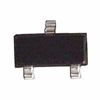
MMBFJ108 Fairchild Semiconductor, MMBFJ108 Datasheet - Page 3

MMBFJ108
Manufacturer Part Number
MMBFJ108
Description
IC SWITCH N-CHAN 25V 80MA SSOT3
Manufacturer
Fairchild Semiconductor
Datasheet
1.J109_D26Z.pdf
(7 pages)
Specifications of MMBFJ108
Current - Drain (idss) @ Vds (vgs=0)
80mA @ 15V
Fet Type
N-Channel
Voltage - Breakdown (v(br)gss)
25V
Voltage - Cutoff (vgs Off) @ Id
3V @ 10nA
Resistance - Rds(on)
8 Ohm
Mounting Type
Surface Mount
Package / Case
TO-236-3, SC-59, SOT-23-3
Power - Max
350mW
Configuration
Single
Transistor Polarity
N-Channel
Power Dissipation
350 mW
Gate-source Breakdown Voltage
- 25 V
Gate-source Cutoff Voltage
- 10 V
Drain Current (idss At Vgs=0)
10 mA
Resistance Drain-source Rds (on)
8 Ohms
Maximum Operating Temperature
+ 150 C
Maximum Drain Gate Voltage
25 V
Minimum Operating Temperature
- 55 C
Mounting Style
SMD/SMT
Breakdown Voltage Vbr
-25V
Gate-source Cutoff Voltage Vgs(off) Max
-10V
Power Dissipation Pd
350mW
Operating Temperature Range
-55°C To +150°C
No. Of Pins
3
Current Rating
80mA
Rohs Compliant
Yes
Lead Free Status / RoHS Status
Lead free / RoHS Compliant
Available stocks
Company
Part Number
Manufacturer
Quantity
Price
Company:
Part Number:
MMBFJ108
Manufacturer:
MOLEX
Quantity:
4 000
Part Number:
MMBFJ108
Manufacturer:
FAIRCHILD/仙童
Quantity:
20 000
©2002 Fairchild Semiconductor Corporation
Typical Characteristics
100
100
100
V
80
60
40
20
10
50
20
10
GS
0
5
2
1
Figure 5. Normalized Drain Resistance vs
0
0
0
/V
Normalized Drain Resistance
V
GS(off)
r
V
Figure 1. Common Drain-Source
Figure 3. Common Drain-Source
DS
f = 0.1 - 1.0 MHz
GS(off)
GS
Common Drain-Source
Common Drain-Source
=
V
= 0 V
V
- NORMALIZED GATE-SOURCE VOLTAGE (V)
1 -
DS
0.2
0.4
GS
-4
@ 5.0V, 10 A
________
- DRAIN-SOURCE VOLTAGE (V)
vs Bias Voltage
- GATE-SOURCE VOLTAGE (V)
V
r
V
- 5.0 V
DS
GS
Bias Voltage
GS(off)
- 4.0 V
0.4
0.8
-8
C
rss
C
iss
- 1.0 V
(V
DS
(V
DS
-12
0.6
1.2
= 0 )
TYP V
- 2.0 V
= 5.0V)
T = 25 캜 캜 캜 캜
GS(off)
A
-16
0.8
1.6
- 3.0 V
= - 5.0 V
C
-20
1
2
100
100
50
40
30
20
10
50
10
_
0
50
10
5
0.1
5
1
0.01 0.03
0
Figure 6. Noise Voltage vs Frequency
I
TYP V
V
BW = 6.0 Hz @ f = 10 Hz, 100 Hz
V
DSS
Noise Voltage vs Frequency
DG
GS(off)
V
I
Figure 4. Common Drain-Source
r
Figure 2. Parameter Interactions
GS (OFF)
D
@ V
= 0.21 @ f
DS
Parameter Interactions
= 10V
Common Drain-Source
T = 25 캜 캜 캜 캜
= 10 mA
V
@ V
GS(off)
@ V
A
DS
DS
V
1
= 5.0V, V
DS
GS
- DRAIN-SOURCE VOLTAGE (V)
DS
0.1
= 100mV, V
- GATE CUTOFF VOLTAGE (V)
_
= - 0.7 V
C
= 5.0V, I
= 0 V
f - FREQUENCY (kHz)
0.5
1.0 kHz
- 0.1 V
GS
- 0.2 V
= 0 PULSED
2
r
D
0.5 1
GS
DS
_
= 3.0 nA
1
= 0
I
DSS
2
3
- 0.3 V
I
D
= 1.0 mA
10
_
- 0.4 V - 0.5 V
5
4
Rev. B1, November 2002
_
10
1,000
500
100
50
10
100
5


