PN4118 Fairchild Semiconductor, PN4118 Datasheet
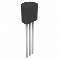
JFET SWITCH N-CHAN TO-92

PN4118

Manufacturer Part Number
PN4118
Description
JFET SWITCH N-CHAN TO-92
Manufacturer
Fairchild Semiconductor
Datasheet

Specifications of PN4118

Current - Drain (idss) @ Vds (vgs=0)
80µA @ 10V
Fet Type
N-Channel
Voltage - Breakdown (v(br)gss)
40V
Voltage - Cutoff (vgs Off) @ Id
1V @ 1nA
Input Capacitance (ciss) @ Vds
3pF @ 10V
Mounting Type
Through Hole
Package / Case
TO-92-3 (Standard Body), TO-226
Power - Max
350mW
Configuration
Single
Transistor Polarity
N-Channel
Power Dissipation
350 mW
Gate-source Breakdown Voltage
- 40 V
Gate-source Cutoff Voltage
- 3 V
Drain Current (idss At Vgs=0)
15 mA
Forward Transconductance Gfs (max / Min)
0.00008 S to 0.00025 S
Maximum Operating Temperature
+ 150 C
Maximum Drain Gate Voltage
40 V
Minimum Operating Temperature
- 55 C
Mounting Style
Through Hole
Lead Free Status / RoHS Status
Lead free / RoHS Compliant

Available stocks

Company
Part Number
Manufacturer
Quantity
Price
Part Number:
PN4118
Manufacturer:
SI
Quantity:
758
Part Number:
PN4118
Manufacturer:
FAIRCHILD/仙童
Quantity:
20 000
Part Number:
PN4118A
Manufacturer:
FAIRCHILD
Quantity:
20 000
1997 Fairchild Semiconductor Corporation
V
V
I
T
P
R
R
Symbol
GF
Symbol
J
DG
GS
D
*
NOTES:
1) These ratings are based on a maximum junction temperature of 150 degrees C.
2) These are steady state limits. The factory should be consulted on applications involving pulsed or low duty cycle operations.
Thermal Characteristics
*
N-Channel Switch
This device is designed for low current DC and audio applications.
These devices provide excellent performance as input stages for
sub-picoamp instrumentation or any high impedance signal
sources. Sourced from Process 53.
Absolute Maximum Ratings*
JC
JA
,T
These ratings are limiting values above which the serviceability of any semiconductor device may be impaired.
Device mounted on FR-4 PCB 1.6" X 1.6" X 0.06."
stg
Drain-Gate Voltage
Gate-Source Voltage
Forward Gate Current
Operating and Storage Junction Temperature Range
Total Device Dissipation
Thermal Resistance, Junction to Case
Thermal Resistance, Junction to Ambient
G
Derate above 25 C
S
D
PN4117
PN4118
PN4119
Characteristic
TO-92
Parameter
TA = 25°C unless otherwise noted
Mark: 61A / 61C / 61E
PN4117-4119
MMBF4117
MMBF4118
MMBF4119
SOT-23
350
125
357
2.8
G
NOTE: Source & Drain
are interchangeable
Max
-55 to +150
*MMBF4117-4119
Value
D
- 40
40
50
225
556
1.8
S
Units
mA
V
V
C
mW/ C
Units
mW
C/W
C/W

Related parts for PN4118

PN4118 Summary of contents

Page 1

... PN4117 PN4118 PN4119 N-Channel Switch This device is designed for low current DC and audio applications. These devices provide excellent performance as input stages for sub-picoamp instrumentation or any high impedance signal sources. Sourced from Process 53. Absolute Maximum Ratings* Symbol V Drain-Gate Voltage DG V Gate-Source Voltage ...

Page 2

Electrical Characteristics Symbol Parameter OFF CHARACTERISTICS V Gate-Source Breakdown Voltage (BR)GSS I Gate Reverse Current GSS V Gate-Source Cutoff Voltage GS(off) ON CHARACTERISTICS I Zero-Gate Voltage Drain Current* DSS SMALL-SIGNAL CHARACTERISTICS Common-Source Forward g fs Transconductance Common-Source Output g oss ...

Page 3

Typical Characteristics Parameter Interactions Transfer Characteristics Transfer Characteristics N-Channel Switch (continued) Transfer Characteristics Transfer Characteristics Transfer Characteristics ...

Page 4

Typical Characteristics Leakage Current vs. Voltage Output Conductance vs. Drain Current Transconductance vs. Drain Current (continued) Common Drain-Source Capacitance vs. Voltage Noise Voltage vs. Frequency N-Channel Switch (continued) 5 ...

Page 5

... TRADEMARKS The following are registered and unregistered trademarks Fairchild Semiconductor owns or is authorized to use and is not intended exhaustive list of all such trademarks. ACEx™ FASTr™ Bottomless™ GlobalOptoisolator™ CoolFET™ GTO™ CROSSVOLT™ HiSeC™ DOME™ ISOPLANAR™ ...

Related keywords