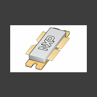
BLF888 NXP Semiconductors, BLF888 Datasheet - Page 6

BLF888
Manufacturer Part Number
BLF888
Description
RF MOSFET Small Signal 500W, 470-860MHz
Manufacturer
NXP Semiconductors
Datasheet
1.BLF888.pdf
(17 pages)
Specifications of BLF888
Configuration
Dual Common Source
Transistor Polarity
N-Channel
Resistance Drain-source Rds (on)
0.105 Ohms
Drain-source Breakdown Voltage
104 V
Gate-source Breakdown Voltage
11 V
Maximum Operating Temperature
+ 200 C
Mounting Style
SMD/SMT
Minimum Operating Temperature
- 65 C
Package / Case
SOT502B
Lead Free Status / RoHS Status
Lead free / RoHS Compliant
Other names
934062101112
Available stocks
Company
Part Number
Manufacturer
Quantity
Price
Company:
Part Number:
BLF888A
Manufacturer:
XYSEMI
Quantity:
12 000
Part Number:
BLF888A
Manufacturer:
NXP/恩智浦
Quantity:
20 000
Company:
Part Number:
BLF888AS
Manufacturer:
NXP
Quantity:
5 000
NXP Semiconductors
BLF888
Product data sheet
Fig 4.
Fig 6.
(dB)
G
(dB)
G
p
p
22
20
18
16
14
12
10
24
22
20
18
16
14
12
10
8
400
0
V
narrowband 860 MHz test circuit.
DVB-T power gain and intermodulation
distortion shoulder as function of load power;
typical values
P
common source broadband test circuit as described in
Section
2-Tone power gain and drain efficiency as
function of frequency; typical values
DS
L(AV)
= 50 V; I
50
= 250 W; V
7.1.2 DVB-T
7.2.1 2-Tone
500
8.
7.2 Broadband RF figures
100
Dq
IMD
G
η
G
= 1.3 A; measured in a common source
D
p
p
600
DS
150
shldr
= 50 V; I
200
700
Dq
250
= 1.3 A; measured in a
800
All information provided in this document is subject to legal disclaimers.
001aak643
001aak645
300
f (MHz)
P
L
(W)
350
900
Rev. 5 — 21 January 2011
0
−10
−20
−30
−40
−50
−60
60
55
50
45
40
35
30
25
20
IMD
(dBc)
(%)
η
shldr
D
Fig 5.
Fig 7.
(dB)
G
PAR
(dB)
p
12
10
24
22
20
18
16
14
12
10
8
6
4
2
0
8
400
0
V
narrowband 860 MHz test circuit.
DVB-T peak-to-average ratio and drain
efficiency as function of load power;
typical values
P
common source broadband test circuit as described in
Section
2-Tone power gain and third order
intermodulation distortion as function of
frequency; typical values
DS
L(AV)
= 50 V; I
50
= 250 W; V
500
8.
G
IMD3
100
p
Dq
= 1.3 A; measured in a common source
600
DS
150
UHF power LDMOS transistor
= 50 V; I
200
700
PAR
η
Dq
D
250
= 1.3 A; measured in a
800
© NXP B.V. 2011. All rights reserved.
001aak644
001aak646
BLF888
300
f (MHz)
P
L
(W)
350
900
70
50
30
10
−10
−30
−50
−10
−15
−20
−25
−30
−35
−40
−45
−50
(%)
η
D
IMD3
(dBc)
6 of 17


