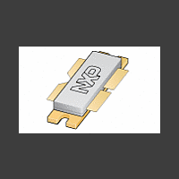
BLF888 NXP Semiconductors, BLF888 Datasheet - Page 3

BLF888
Manufacturer Part Number
BLF888
Description
RF MOSFET Small Signal 500W, 470-860MHz
Manufacturer
NXP Semiconductors
Datasheet
1.BLF888.pdf
(17 pages)
Specifications of BLF888
Configuration
Dual Common Source
Transistor Polarity
N-Channel
Resistance Drain-source Rds (on)
0.105 Ohms
Drain-source Breakdown Voltage
104 V
Gate-source Breakdown Voltage
11 V
Maximum Operating Temperature
+ 200 C
Mounting Style
SMD/SMT
Minimum Operating Temperature
- 65 C
Package / Case
SOT502B
Lead Free Status / RoHS Status
Lead free / RoHS Compliant
Other names
934062101112
Available stocks
Company
Part Number
Manufacturer
Quantity
Price
Company:
Part Number:
BLF888A
Manufacturer:
XYSEMI
Quantity:
12 000
Part Number:
BLF888A
Manufacturer:
NXP/恩智浦
Quantity:
20 000
Company:
Part Number:
BLF888AS
Manufacturer:
NXP
Quantity:
5 000
NXP Semiconductors
5. Thermal characteristics
Table 5.
[1]
6. Characteristics
Table 6.
T
[1]
[2]
Table 7.
T
BLF888
Product data sheet
Symbol
R
Symbol
V
V
I
I
I
g
R
C
C
C
Symbol
2-Tone, class AB
V
I
P
P
G
IMD3
DVB-T (8k OFDM)
V
I
P
G
DSS
DSX
GSS
Dq
Dq
j
h
fs
D
(BR)DSS
GS(th)
DS
L(PEP)
L(AV)
DS
L(AV)
th(j-c)
DS(on)
iss
oss
rss
p
p
= 25
= 25
R
I
Capacitance values without internal matching.
D
th(j-c)
is the drain current.
C unless otherwise specified.
C unless otherwise specified.
is measured under RF conditions.
Thermal characteristics
DC characteristics
RF characteristics
Parameter
thermal resistance from junction to case
third-order intermodulation distortion
Parameter
drain-source breakdown voltage
gate-source threshold voltage
drain leakage current
drain cut-off current
gate leakage current
forward transconductance
drain-source on-state resistance
input capacitance
output capacitance
reverse transfer capacitance
Parameter
drain-source voltage
quiescent drain current
peak envelope power load power
average output power
power gain
drain efficiency
drain-source voltage
quiescent drain current
average output power
power gain
All information provided in this document is subject to legal disclaimers.
Rev. 5 — 21 January 2011
Conditions
V
V
V
V
V
V
V
V
V
V
Conditions
total device
total device
GS
DS
GS
GS
GS
DS
GS
GS
GS
GS
= 10 V; I
= 10 V; I
= 0 V; I
= 0 V; V
= V
= 10 V; V
= V
= 0 V; V
= 0 V; V
= 0 V; V
GS(th)
GS(th)
D
Conditions
T
DS
DS
DS
DS
D
D
= 2.7 mA
+ 3.75 V; V
+ 3.75 V; I
case
DS
= 270 mA
= 13.5 A
= 50 V
= 50 V; f = 1 MHz
= 50 V; f = 1 MHz
= 50 V; f = 1 MHz
= 0 V
= 80 C; P
D
DS
= 9.5 A
= 10 V
L(AV)
= 110 W
UHF power LDMOS transistor
[1]
[1]
[1]
[1]
[2]
[2]
[2]
Min
104
1.4
-
-
-
-
-
-
-
-
Min
-
-
500
250
18
42
-
-
-
110
18
Typ
-
1.9
-
43
-
17
105
205
65
2.2
Typ
50
1.3
-
-
19
46
32
50
1.3
-
19
© NXP B.V. 2011. All rights reserved.
[1]
BLF888
Max
-
2.4
2.8
-
280
-
-
-
-
-
Max
-
-
-
-
-
-
28
-
-
-
-
Typ
0.24
Unit
V
V
A
A
nA
S
m
pF
pF
pF
Unit
V
A
W
W
dB
%
dBc
V
A
W
dB
Unit
K/W
3 of 17


