ADNS-2610 Avago Technologies US Inc., ADNS-2610 Datasheet - Page 6
ADNS-2610
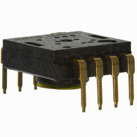
Manufacturer Part Number
ADNS-2610
Description
SENSOR OPTICAL MOUSE 8-DIP
Manufacturer
Avago Technologies US Inc.
Datasheet
1.ADNK-2610.pdf
(27 pages)
Specifications of ADNS-2610
Lead Free Status / RoHS Status
Lead free / RoHS Compliant
Lead Free Status / RoHS Status
Lead free / RoHS Compliant, Lead free / RoHS Compliant
Other names
516-1843
ADNS-2610
ADNS-2610


Absolute Maximum Ratings
Parameter
Storage Temperature
Operating Temperature T
Lead Solder Temp
Supply Voltage
ESD
Input Voltage
Input Voltage
Recommended Operating Conditions
Parameter
Operating Temperature
Power Supply Voltage
Power Supply Rise Time
Supply Noise
Clock Frequency
Serial Port Clock Frequency
Resonator Impedance
Distance from Lens
Reference Plane to Surface
Speed
Acceleration
Light Level onto IC
SDIO Read Hold Time
SDIO Serial
Write-write Time
SDIO Serial
Write-read Time
SDIO Serial
Read-write Time
SDIO Serial
Read-read Time
Data Delay after
PD deactivated
SDIO Write Setup Time
Frame Rate
6
Symbol
T
V
V
V
A
S
DD
IN
IN
Symbol
T
V
V
V
f
SCLK
X
Z
S
A
t
t
t
t
t
t
t
FR
IRR
CLK
HOLD
SWW
SWR
SRW
SRR
COMPUTE
SETUP
A
DD
RT
N
RES
INC
Minimum
-40
-15
-0.5
-0.5
-0.5
Minimum
0
4.1
23.0
80
100
100
100
3.1
2.3
0
100
250
250
60
Maximum
85
55
260
5.5
2
V
3.6
DD
Typical
5.0
24.0
2.4
+0.5
Maximum
40
5.5
100
100
25.0
f
55
2.5
12
0.25
25,000
30,000
1500
CLK
Units
°C
°C
°C
V
KV
V
V
/12
Notes
For 10 seconds, 1.6 mm below seating plane
All pins, human body model MIL 883 Method 3015
SDIO, CLK, LED_CNTL
OSC_IN, OSC_OUT, REFA
Units
°C
Volts
ms
mV
MHz
MHz
Ω
mm
in/sec
g
mW/m
µs
µs
µs
ns
ns
ms
ns
frames/s
2
Notes
Register values retained for voltage
transients below 4.10V but greater
than 3.9V
Peak to peak within 0-100 MHz
bandwidth
Set by ceramic resonator
Results in ±0.2 mm DOF
(See Figure 9)
@ frame rate = 1500 fps
@ frame rate = 1500 fps
λ = 639 nm
λ = 875 nm
Hold time for valid data
(Refer to Figure 22)
Time between two write commands
(Refer to Figure 25)
Time between write and read
operation (Refer to Figure 26)
Time between read and write
operation (Refer to Figure 27)
Time between two read commands
(Refer to Figure 26)
After t
data from first image after wakeup
from Power-Down mode. Note that an
additional 75 frames for AGC
stabilization may be required if mouse
movement occurred while Power
Down. (Refer to Figure 10)
Data valid time before the rising of
SCLK (Refer to Figure 20)
COMPUTE
, all registers contain
Related parts for ADNS-2610
Image
Part Number
Description
Manufacturer
Datasheet
Request
R

Part Number:
Description:
Optical Mouse Sensor,DIP
Manufacturer:
Avago Technologies US Inc.
Datasheet:

Part Number:
Description:
Optical Mouse Sensor,DIP
Manufacturer:
Avago Technologies US Inc.
Datasheet:

Part Number:
Description:
Trim Lens For ADNS-3530
Manufacturer:
Avago Technologies US Inc.
Datasheet:

Part Number:
Description:
8 DIP SFF Navigation Sensor
Manufacturer:
Avago Technologies US Inc.
Datasheet:

Part Number:
Description:
Trim Lens For ADNS-5090
Manufacturer:
Avago Technologies US Inc.
Datasheet:

Part Number:
Description:
BLACK CLIP FOR ADNS-5000
Manufacturer:
Avago Technologies US Inc.
Datasheet:
Part Number:
Description:
Lens For ADNS-7630
Manufacturer:
Avago Technologies US Inc.
Datasheet:

Part Number:
Description:
Optical Mouse Sensor,DIP
Manufacturer:
Avago Technologies US Inc.
Datasheet:
Part Number:
Description:
Optical Mouse Sensor,DIP
Manufacturer:
Avago Technologies US Inc.
Datasheet:
Part Number:
Description:
Low Power Wireless LED Sensor
Manufacturer:
Avago Technologies US Inc.
Datasheet:

Part Number:
Description:
OPTOCOUPLER GATE DRV 2A 16-SOIC
Manufacturer:
Avago Technologies US Inc.
Datasheet:
Part Number:
Description:
OPTOCOUPLER 2CH 2.5A 16-SOIC
Manufacturer:
Avago Technologies US Inc.
Datasheet:

Part Number:
Description:
OPTOCOUPLER GATE DRV 0.4A 16SOIC
Manufacturer:
Avago Technologies US Inc.
Datasheet:

Part Number:
Description:
OPTOCOUPLER 2.0A 250KHZ 8-DIP
Manufacturer:
Avago Technologies US Inc.
Datasheet:

Part Number:
Description:
OPTOCOUPLER 2.0A 250KHZ GW 8-SMD
Manufacturer:
Avago Technologies US Inc.
Datasheet: