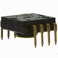
ADNS-2610 Avago Technologies US Inc., ADNS-2610 Datasheet - Page 16

ADNS-2610
Manufacturer Part Number
ADNS-2610
Description
SENSOR OPTICAL MOUSE 8-DIP
Manufacturer
Avago Technologies US Inc.
Datasheet
1.ADNK-2610.pdf
(27 pages)
Specifications of ADNS-2610
Lead Free Status / RoHS Status
Lead free / RoHS Compliant
Lead Free Status / RoHS Status
Lead free / RoHS Compliant, Lead free / RoHS Compliant
Other names
516-1843
ADNS-2610
ADNS-2610
Error Detection and Recovery
1. The ADNS-2610 and the microcontroller might get out
2. The ADNS-2610 has a transaction timer for the serial
3. Invalid addresses:
4. Collision detection on SDIO
5. In case of synchronization failure, both the ADNS-2610
6. The microcontroller can verify a successful write opera-
7. The microcontroller can verify the synchronization of
SDIO
Figure 28. Power-up serial port sequence.
16
V
SCK
DD
of synchronization due to ESD events, power supply
droops or microcontroller firmware flaws.
port. If the sixteenth SCK rising edge is spaced more
than approximately 90 milliseconds from the first SCK
edge of the current transaction, the serial port will
reset.
– Writing to an invalid address will have no effect.
– The only time that the ADNS-2610 drives the SDIO line
and the microcontroller may drive SDIO. The ADNS-
2610 can withstand 30 mA of short circuit current and
will withstand infinite duration short circuit condi-
tions.
tion by issuing a read command to the same address
and comparing the written data to the read data.
the serial port by periodically reading the product ID
from status register (Address: 0x01).
Reading from an invalid address will return all ze-
ros.
is during a READ operation. To avoid data collisions,
the microcontroller should relinquish SDIO before the
falling edge of SCK after the last address bit. Then the
ADNS-2610 begins to drive SDIO after the next rising
edge of SCK. Next, the ADNS-2610 relinquishes SDIO
within 160 ns of the falling SCK edge after the last
data bit. The microcontroller can begin driving SDIO
any time after that. In order to maintain low power
consumption in normal operation or when the PD bit
is set high, the microcontroller should not leave SDIO
floating until the next transmission (although that will
not cause any communication difficulties).
Problem Area
Address ≠ 0x01
Data ≠ 0x0b000XXXXX
Notes on Power-up and the Serial Port
The sequence in which V
powerup can affect the operation of the serial port. The
diagram below shows what can happen shortly after
powerup when the microprocessor tries to read data from
the serial port.
This diagram shows the V
point the microcontroller starts its program, sets the
SCK and SDIO lines to be outputs, and sets them high.
Then, the microcontroller waits to ensure the ADNS-
2610 has powered up and is ready to communicate. The
microprocessor then tries to read from location 0x01,
Status register, and is expecting a value of 0x0b000XXXXX
– where X is in DON’T CARE state. If it receives this value,
it then knows that the communication to the ADNS-2610
is operational.
The problem occurs if the ADNS-2610 powers up before
the microprocessor sets the SCK and SDIO lines to be
outputs and high. The ADNS-2610 sees the raising of the
SCK as a valid rising edge, and clocks in the state of the
SDIO as the first bit of the address (sets either a read or a
write depending upon the state).
In the case of a SDIO low, a read operation will start. When
the microprocessor actually begins to send the address,
the ADNS-2610 already has the first bit of an address.
When the seventh bit is sent by the microprocessor, the
ADNS-2610 has a valid address, and drives the SDIO line
high within 250 ns (see detail “A” in Figure 21 and Figure
22). This results in a bus fight for SDIO. Since the address
is wrong, the data sent back will be incorrect.
In the case of SDIO high, a write operation will start. The
address and data will be out of synchronization, causing
the wrong data written to the wrong address.
Solution
There is one way to solve the problem, which is waiting
for the serial port timer to time out.
DD
DD
, SCK and SDIO are set during
rising to valid levels, at some


