AD9788-EBZ Analog Devices Inc, AD9788-EBZ Datasheet - Page 51
AD9788-EBZ
Manufacturer Part Number
AD9788-EBZ
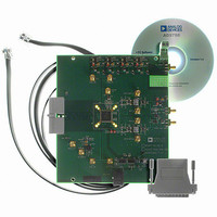
Description
BOARD EVAL FOR AD9788
Manufacturer
Analog Devices Inc
Series
TxDAC®r
Datasheet
1.AD9785BSVZ.pdf
(64 pages)
Specifications of AD9788-EBZ
Design Resources
Powering the AD9788 Using ADP2105 for Increased Efficiency (CN0141)
Number Of Dac's
2
Number Of Bits
16
Outputs And Type
2, Differential
Sampling Rate (per Second)
800M
Data Interface
Serial
Settling Time
22ms
Dac Type
Current
Voltage Supply Source
Analog and Digital
Operating Temperature
-40°C ~ 85°C
Utilized Ic / Part
AD9788
Silicon Manufacturer
Analog Devices
Application Sub Type
DAC
Kit Application Type
Data Converter
Silicon Core Number
AD9788
Kit Contents
Board
Development Tool Type
Hardware - Eval/Demo Board
Lead Free Status / RoHS Status
Lead free / RoHS Compliant


There are two output signals on each auxiliary DAC. One signal
is designated P, the other N. The sign bit in each auxiliary DAC
control register (Bit 15) controls whether the P side or the N side
of the auxiliary DAC is turned on. Only one side of the auxiliary
DAC is active at a time. The auxiliary DAC structure is shown
in Figure 71.
The magnitude of the auxiliary DAC 1 current is controlled by
the auxiliary DAC 1 control register (Register 0x06), and the
magnitude of the auxiliary DAC 2 current is controlled by the
auxiliary DAC 2 control register (Register 0x08). These auxiliary
DACs have the ability to source or sink current. This selection is
programmable via Bit 14 in either auxiliary DAC control register.
(SOURCE)
V
0 TO 2mA
0 TO 2mA
BIAS
(SINK)
Figure 71. Auxiliary DAC Structure
SOURCE/
SINK
Figure 73. Typical Use of Auxiliary DACs DC Coupling to Quadrature Modulator with DC Shift
P/N
Figure 72. Typical Use of Auxiliary DACs AC Coupling to Quadrature Modulator
25Ω TO 50Ω
I DAC
DAC1 OR
I OR Q DAC
AUX_P
AUX_N
DAC2
AUX
25Ω TO 50Ω
0.1µF
0.1µF
25Ω TO 50Ω
Q DAC
OPTIONAL
FILTERING
PASSIVE
Rev. A | Page 51 of 64
OPTIONAL
FILTERING
PASSIVE
MODULATOR V+
QUADRATURE
0.1µF
0.1µF
The choice of sinking or sourcing should be made at circuit
design time. There is no advantage to switching between
sourcing and sinking current after the circuit is in place.
The auxiliary DACs can be used for local oscillator (LO) cancel-
lation when the DAC output is followed by a quadrature modu-
lator. This LO feedthrough is caused by the input referred dc
offset voltage of the quadrature modulator (and the DAC output
offset voltage mismatch) and can degrade system performance.
Typical DAC-to-quadrature modulator interfaces are shown in
Figure 72 and Figure 73. Often, the input common-mode
voltage for the modulator is much higher than the output
compliance range of the DAC, so that ac coupling or a dc level
shift is necessary. If the required common-mode input voltage
on the quadrature modulator matches that of the DAC, then the
dc blocking capacitors in Figure 72 can be removed.
A low-pass or band-pass passive filter is recommended when
spurious signals from the DAC (distortion and DAC images) at
the quadrature modulator inputs can affect system performance.
Placing the filter at the location shown in Figure 72 and Figure 73
allows easy design of the filter, as the source and load impedances
can easily be designed close to 50 Ω.
OPTIONAL
FILTERING
PASSIVE
QUAD MOD
I INPUTS
DAC1
AUX
25Ω TO 50Ω
MODULATOR V+
QUADRATURE
QUAD MOD
I AND Q INPUTS
QUAD MOD
Q INPUTS
DAC2
AUX
AD9785/AD9787/AD9788
Related parts for AD9788-EBZ
Image
Part Number
Description
Manufacturer
Datasheet
Request
R

Part Number:
Description:
Dual 16B, 1.0 GSPS TxDAC
Manufacturer:
Analog Devices Inc
Datasheet:

Part Number:
Description:
±1.7g Dual-Axis IMEMS Accelerometer Evaluation Board
Manufacturer:
Analog Devices Inc
Datasheet:
Part Number:
Description:
Inertial Sensor Evaluation System
Manufacturer:
Analog Devices Inc
Datasheet:
Part Number:
Description:
Manufacturer:
Analog Devices Inc
Datasheet:
Part Number:
Description:
Manufacturer:
Analog Devices Inc
Datasheet:
Part Number:
Description:
Manufacturer:
Analog Devices Inc
Datasheet:
Part Number:
Description:
Manufacturer:
Analog Devices Inc
Datasheet:
Part Number:
Description:
Manufacturer:
Analog Devices Inc
Datasheet:
Part Number:
Description:
Manufacturer:
Analog Devices Inc
Datasheet:
Part Number:
Description:
Manufacturer:
Analog Devices Inc
Datasheet:
Part Number:
Description:
Manufacturer:
Analog Devices Inc
Datasheet:
Part Number:
Description:
Manufacturer:
Analog Devices Inc
Datasheet:
Part Number:
Description:
Manufacturer:
Analog Devices Inc
Datasheet: