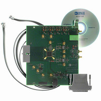
AD9788-EBZ Analog Devices Inc, AD9788-EBZ Datasheet - Page 27

AD9788-EBZ
Manufacturer Part Number
AD9788-EBZ
Description
BOARD EVAL FOR AD9788
Manufacturer
Analog Devices Inc
Series
TxDAC®r
Datasheet
1.AD9785BSVZ.pdf
(64 pages)
Specifications of AD9788-EBZ
Design Resources
Powering the AD9788 Using ADP2105 for Increased Efficiency (CN0141)
Number Of Dac's
2
Number Of Bits
16
Outputs And Type
2, Differential
Sampling Rate (per Second)
800M
Data Interface
Serial
Settling Time
22ms
Dac Type
Current
Voltage Supply Source
Analog and Digital
Operating Temperature
-40°C ~ 85°C
Utilized Ic / Part
AD9788
Silicon Manufacturer
Analog Devices
Application Sub Type
DAC
Kit Application Type
Data Converter
Silicon Core Number
AD9788
Kit Contents
Board
Development Tool Type
Hardware - Eval/Demo Board
Lead Free Status / RoHS Status
Lead free / RoHS Compliant
The data synchronization control register (DSCR) comprises two bytes located at Address 0x02.
Table 12. Data Synchronization Control Register (DSCR)
Address
0x02
Bit
[15:11]
[10:7]
[6]
[5]
[4]
[3]
[2]
[1]
[0]
Name
DATACLK Delay [4:0]
Data Timing Margin [3:0]
LVDS data clock enable
DATACLK invert
DATACLK delay enable
Data timing mode
Set high
Data sync polarity
Reserved
Description
Controls the amount of delay applied to the output data clock signal. The minimum delay
corresponds to the 00000 state, and the maximum delay corresponds to the 11111 state.
The minimum delay is 0.7 ns and the maximum delay is 6.5 ns. The incremental delay is
190 ps and corresponds to an incremental change in the data clock delay bits.
The data timing margin bits control the amount of delay applied to the data and clock
signals used for checking setup and hold times, respectively, on the input data ports, with
respect to the internal data assembler clock. The minimum delay corresponds to the 0000
state, and the maximum delay corresponds to the 1111 state. The delays are 190 ps.
0: Default. When the LVDS data clock enable bit is cleared, the SYNC_O+ and SYNC_O−
LVDS pad cells are driven by the multichip synchronization logic.
1: When the LVDS data clock enable bit is set, the SYNC_O+ and SYNC_O− LVDS pad cells
are driven by the signal that drives the CMOS DATACLK output pad.
0: Default. When the data clock invert bit is cleared, the DATACLK signal is in phase with
the clock that samples the data into the part.
1: When the DATACLK invert bit is set, the DATACLK signal is inverted from the clock that
samples the data into the part.
0: Default. When the DATACLK delay enable bit is cleared, the data port input
synchronization function is effectively inactive and the delay is bypassed.
1: When the DATACLK delay enable bit is set, the data port input synchronization function
is active and controlled by the data delay mode bits. The data output clock is routed
through the delay cell.
Determines the timing optimization mode. See the Optimizing the Data Input Timing
section for details.
0: Manual timing optimization mode
1: Automatic timing optimization mode
This bit should always be set high.
0: Default. The digital input data sampling edge is aligned with the falling edge of DCI.
1: The digital input data sampling edge is aligned with the rising edge of DCI.
Used only in slave mode (see the MSCR register, Address 0x03, Bit 16).
Reserved for future use.
Rev. A | Page 27 of 64
AD9785/AD9787/AD9788


