AD9788-EBZ Analog Devices Inc, AD9788-EBZ Datasheet - Page 28
AD9788-EBZ
Manufacturer Part Number
AD9788-EBZ
Description
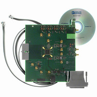
BOARD EVAL FOR AD9788
Manufacturer
Analog Devices Inc
Series
TxDAC®r
Datasheet
1.AD9785BSVZ.pdf
(64 pages)
Specifications of AD9788-EBZ
Design Resources
Powering the AD9788 Using ADP2105 for Increased Efficiency (CN0141)
Number Of Dac's
2
Number Of Bits
16
Outputs And Type
2, Differential
Sampling Rate (per Second)
800M
Data Interface
Serial
Settling Time
22ms
Dac Type
Current
Voltage Supply Source
Analog and Digital
Operating Temperature
-40°C ~ 85°C
Utilized Ic / Part
AD9788
Silicon Manufacturer
Analog Devices
Application Sub Type
DAC
Kit Application Type
Data Converter
Silicon Core Number
AD9788
Kit Contents
Board
Development Tool Type
Hardware - Eval/Demo Board
Lead Free Status / RoHS Status
Lead free / RoHS Compliant


AD9785/AD9787/AD9788
The multichip synchronization register (MSCR) comprises four bytes located at Address 0x03.
Table 13. Multichip Synchronization Register (MSCR)
Address
0x03
[31:27]
[26]
[25]
[24]
[23:19]
[18]
[17]
[16]
[15:11]
[10]
[9]
[8]
[7:4]
[3:0]
Bit
Name
Correlate Threshold
[4:0]
SYNC_I enable
SYNC_O enable
Set low
SYNC_I Delay [4:0]
Sync error check mode
Set low
DATACLK input
SYNC_O Delay [4:0]
Set high
SYNC_O polarity
Sync loopback enable
Clock State [3:0]
Sync Timing Margin
[3:0]
Description
Sets the threshold for determining if the received synchronization data can be demodulated
accurately. A smaller threshold value makes the demodulator more noise immune; however,
the system becomes more susceptible to false locks (or demodulation errors).
0: Default. The synchronization receive logic is disabled.
1: The synchronization receive logic is enabled.
0: Default. The output synchronization pulse generation logic is disabled.
1: The output synchronization pulse generation logic is enabled.
This bit should always be set low.
This value programs the value of the delay line of the SYNC_I signal. The delay line resolution
is 80 ps per step.
00000: nominal delay
00001: adds 80 ps delay to SYNC_I
00010: adds 160 ps delay to SYNC_I
…
11111: adds 2480 ps delay to SYNC_I
Specifies the synchronization pulse error check mode.
0: Manual error check
1: Automatic continuous error check
This bit should always be set low.
0: Default. Slave mode is disabled.
1: Slave mode is enabled. Pin 37 functions as an input for the DATACLK signal, called DCI
(DATACLK input) in this mode. Depending on the state of Bit 1 in the DSCR register (Address
0x02), the sampling edge (where the data is latched into the AD9785/AD9787/AD9788) can
be programmed to be aligned with either the rising or falling edge of DCI. This mode can
only be used with 4× or 8× interpolation.
This value programs the value of the delay line of the SYNC_O signal. The delay of SYNC_O is
relative to REFCLK. The delay line resolution is 80 ps per step.
00000: nominal delay
00001: adds 80 ps delay to SYNC_O
00010: adds 160 ps delay to SYNC_O
…
11111: adds 2480 ps delay to SYNC_O
This bit should always be set high.
0: Default. SYNC_O changes state on the rising edge of DACCLK.
1: SYNC_O is generated on the falling edge of DACCLK.
0: Default. The AD9785/AD9787/AD9788 are not operating in internal loopback mode.
1: If the SYNC_O enable and Sync loopback enable bits are set, the AD9785/AD9787/AD9788
are operating in a mode in which the internal synchronization pulse of the device is used at
the multichip receiver logic and the SYNC_I+ and SYNC_I− input pins are ignored. For proper
operation of the loopback synchronization mode, the synchronization driver enable and
sync enable bits must be set.
This value determines the state of the internal clock generation state machine upon
synchronization.
These bits are the synchronization window delay word. These bits are don’t care if the
synchronization driver enable bit is cleared.
Rev. A | Page 28 of 64
Related parts for AD9788-EBZ
Image
Part Number
Description
Manufacturer
Datasheet
Request
R

Part Number:
Description:
Dual 16B, 1.0 GSPS TxDAC
Manufacturer:
Analog Devices Inc
Datasheet:

Part Number:
Description:
±1.7g Dual-Axis IMEMS Accelerometer Evaluation Board
Manufacturer:
Analog Devices Inc
Datasheet:
Part Number:
Description:
Inertial Sensor Evaluation System
Manufacturer:
Analog Devices Inc
Datasheet:
Part Number:
Description:
Manufacturer:
Analog Devices Inc
Datasheet:
Part Number:
Description:
Manufacturer:
Analog Devices Inc
Datasheet:
Part Number:
Description:
Manufacturer:
Analog Devices Inc
Datasheet:
Part Number:
Description:
Manufacturer:
Analog Devices Inc
Datasheet:
Part Number:
Description:
Manufacturer:
Analog Devices Inc
Datasheet:
Part Number:
Description:
Manufacturer:
Analog Devices Inc
Datasheet:
Part Number:
Description:
Manufacturer:
Analog Devices Inc
Datasheet:
Part Number:
Description:
Manufacturer:
Analog Devices Inc
Datasheet:
Part Number:
Description:
Manufacturer:
Analog Devices Inc
Datasheet:
Part Number:
Description:
Manufacturer:
Analog Devices Inc
Datasheet: