AD9788-EBZ Analog Devices Inc, AD9788-EBZ Datasheet - Page 21
AD9788-EBZ
Manufacturer Part Number
AD9788-EBZ
Description
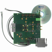
BOARD EVAL FOR AD9788
Manufacturer
Analog Devices Inc
Series
TxDAC®r
Datasheet
1.AD9785BSVZ.pdf
(64 pages)
Specifications of AD9788-EBZ
Design Resources
Powering the AD9788 Using ADP2105 for Increased Efficiency (CN0141)
Number Of Dac's
2
Number Of Bits
16
Outputs And Type
2, Differential
Sampling Rate (per Second)
800M
Data Interface
Serial
Settling Time
22ms
Dac Type
Current
Voltage Supply Source
Analog and Digital
Operating Temperature
-40°C ~ 85°C
Utilized Ic / Part
AD9788
Silicon Manufacturer
Analog Devices
Application Sub Type
DAC
Kit Application Type
Data Converter
Silicon Core Number
AD9788
Kit Contents
Board
Development Tool Type
Hardware - Eval/Demo Board
Lead Free Status / RoHS Status
Lead free / RoHS Compliant


THEORY OF OPERATION
The AD9785/AD9787/AD9788 devices combine many features
that make them very attractive DACs for wired and wireless
communications systems. The dual digital signal path and dual
DAC structure allow an easy interface to common quadrature
modulators when designing single sideband transmitters. The
speed and performance of the AD9785/AD9787/AD9788 allow
wider bandwidths and more carriers to be synthesized than in
previously available DACs. In addition, these devices include
an innovative low power, 32-bit complex NCO that greatly
increases the ease of frequency placement.
The AD9785/AD9787/AD9788 offer features that allow
simplified synchronization with incoming data and between
multiple parts, as well as the capability to phase synchronize
NCOs on multiple devices. Auxiliary DACs are also provided
on chip for output dc offset compensation (for LO compen-
sation in SSB transmitters) and for gain matching (for image
rejection optimization in SSB transmitters). Another innovative
feature in the devices is the digitally programmable output
phase compensation, which increases the amount of image
cancellation capability in SSB (single sideband) transmitters.
TXENABLE
DATACLK
P1D[15:0]
P2D[15:0]
SYNC_O
SYNC_I
16
16
LVDS
LVDS
1
0
DELAY
DELAY
LINE
LINE
DELAY
LINE
FILTER
QUAD
(2×)
HB
SYNCHRONIZATION
FILTER
QUAD
MULTICHIP
(2×)
HB
INTERNAL CLOCK TIMING AND CONTROL LOGIC
FILTER
QUAD
(2×)
HB
PROGRAMMING
REGISTERS
0
1
2
3
3
2
1
0
Figure 42. Functional Block Diagram
16
16
Rev. A | Page 21 of 64
COS
+
SIN
+
SERIAL
+
+
PORT
I/O
NCO
ω
θ
16
32
SERIAL PORT INTERFACE
The AD9785/AD9787/AD9788 serial port is a flexible,
synchronous serial communications port allowing easy
interface to many industry-standard microcontrollers and
microprocessors. The serial I/O is compatible with most
synchronous transfer formats, including both the Motorola®
6905/11 SPI and the Intel® 8051 SSR protocols.
The serial interface allows read/write access to all registers that
configure the AD9785/AD9787/AD9788. MSB first and LSB
first transfer formats are supported. In addition, the serial
interface port can be configured as a single-pin I/O (SDIO),
which allows a 3-wire interface, or two unidirectional pins for
input/output (SDIO/SDO), which enables a 4-wire interface.
One optional pin, SPI_CSB (chip select), allows enabling of
multiple devices on a single bus.
With the AD9785/AD9787/AD9788, the instruction byte
specifies read/write operation and the register address. Serial
operations on the AD9785/AD9787/AD9788 occur only at the
register level, not at the byte level, due to the lack of byte
address space in the instruction byte.
POWER-ON
RESET
SIN(×)
SIN(×)
×
×
PHASE
CORRECTION
0
1
0
1
Q-SCALE
I-SCALE
PLL CONTROL
DAC_CLK
10
AD9785/AD9787/AD9788
Q-OFFSET
I-OFFSET
16
16
0
1
MULTIPLIER
(2× – 16×)
CLOCK
10
10
16-BIT
16-BIT
AUX1
AUX2
DAC1
DAC2
R
CLK
CVR
OUT1_P
OUT1_N
OUT2_P
OUT2_N
VREF
RESET
AUX1_P
AUX1_N
AUX2_P
AUX2_N
REFCLK+
REFCLK–
Related parts for AD9788-EBZ
Image
Part Number
Description
Manufacturer
Datasheet
Request
R

Part Number:
Description:
Dual 16B, 1.0 GSPS TxDAC
Manufacturer:
Analog Devices Inc
Datasheet:

Part Number:
Description:
±1.7g Dual-Axis IMEMS Accelerometer Evaluation Board
Manufacturer:
Analog Devices Inc
Datasheet:
Part Number:
Description:
Inertial Sensor Evaluation System
Manufacturer:
Analog Devices Inc
Datasheet:
Part Number:
Description:
Manufacturer:
Analog Devices Inc
Datasheet:
Part Number:
Description:
Manufacturer:
Analog Devices Inc
Datasheet:
Part Number:
Description:
Manufacturer:
Analog Devices Inc
Datasheet:
Part Number:
Description:
Manufacturer:
Analog Devices Inc
Datasheet:
Part Number:
Description:
Manufacturer:
Analog Devices Inc
Datasheet:
Part Number:
Description:
Manufacturer:
Analog Devices Inc
Datasheet:
Part Number:
Description:
Manufacturer:
Analog Devices Inc
Datasheet:
Part Number:
Description:
Manufacturer:
Analog Devices Inc
Datasheet:
Part Number:
Description:
Manufacturer:
Analog Devices Inc
Datasheet:
Part Number:
Description:
Manufacturer:
Analog Devices Inc
Datasheet: