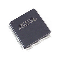
EPM1270GT144I5N Altera, EPM1270GT144I5N Datasheet - Page 47

EPM1270GT144I5N
Manufacturer Part Number
EPM1270GT144I5N
Description
MAX II
Manufacturer
Altera
Datasheet
1.EPM1270GT144I5N.pdf
(88 pages)
Specifications of EPM1270GT144I5N
Family Name
MAX II
Memory Type
Flash
# Macrocells
980
Frequency (max)
1.8797GHz
Propagation Delay Time
10ns
Number Of Logic Blocks/elements
127
# I/os (max)
116
Operating Supply Voltage (typ)
1.8V
In System Programmable
Yes
Operating Supply Voltage (min)
1.71V
Operating Supply Voltage (max)
1.89V
Operating Temp Range
-40C to 100C
Operating Temperature Classification
Industrial
Mounting
Surface Mount
Pin Count
144
Package Type
TQFP
Lead Free Status / Rohs Status
Compliant
Available stocks
Company
Part Number
Manufacturer
Quantity
Price
Company:
Part Number:
EPM1270GT144I5N
Manufacturer:
ALTERA
Quantity:
612
Chapter 3: JTAG and In-System Programmability
In System Programmability
IEEE 1532 Support
Jam Standard Test and Programming Language (STAPL)
Programming Sequence
© October 2008 Altera Corporation
f
The JTAG circuitry and ISP instruction set in MAX II devices is compliant to the IEEE
1532-2002 programming specification. This provides industry-standard hardware and
software for in-system programming among multiple vendor programmable logic
devices (PLDs) in a JTAG chain.
The MAX II 1532 BSDL files will be released on the Altera website when available.
The Jam STAPL JEDEC standard, JESD71, can be used to program MAX II devices
with in-circuit testers, PCs, or embedded processors. The Jam byte code is also
supported for MAX II devices. These software programming protocols provide a
compact embedded solution for programming MAX II devices.
For more information, refer to the
chapter in the MAX II Device Handbook.
During in-system programming, 1532 instructions, addresses, and data are shifted
into the MAX II device through the TDI input pin. Data is shifted out through the TDO
output pin and compared against the expected data. Programming a pattern into the
device requires the following six ISP steps. A stand-alone verification of a
programmed pattern involves only stages 1, 2, 5, and 6. These steps are automatically
executed by third-party programmers, the Quartus II software, or the Jam STAPL and
Jam Byte-Code Players.
1. Enter ISP—The enter ISP stage ensures that the I/O pins transition smoothly from
2. Check ID—Before any program or verify process, the silicon ID is checked. The
3. Sector Erase—Erasing the device in-system involves shifting in the instruction to
4. Program—Programming the device in-system involves shifting in the address,
5. Verify—Verifying a MAX II device in-system involves shifting in addresses,
6. Exit ISP—An exit ISP stage ensures that the I/O pins transition smoothly from ISP
user mode to ISP mode.
time required to read this silicon ID is relatively small compared to the overall
programming time.
erase the device and applying an erase pulse(s). The erase pulse is automatically
generated internally by waiting in the run/test/idle state for the specified erase
pulse time of 500 ms for the CFM block and 500 ms for each sector of the UFM
block.
data, and program instruction and generating the program pulse to program the
flash cells. The program pulse is automatically generated internally by waiting in
the run/test/idle state for the specified program pulse time of 75 µs. This process
is repeated for each address in the CFM and UFM blocks.
applying the verify instruction to generate the read pulse, and shifting out the data
for comparison. This process is repeated for each CFM and UFM address.
mode to user mode.
Using Jam STAPL for ISP via an Embedded Processor
MAX II Device Handbook
3–5


