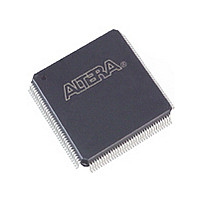
EPM1270GT144I5N Altera, EPM1270GT144I5N Datasheet - Page 28

EPM1270GT144I5N
Manufacturer Part Number
EPM1270GT144I5N
Description
MAX II
Manufacturer
Altera
Datasheet
1.EPM1270GT144I5N.pdf
(88 pages)
Specifications of EPM1270GT144I5N
Family Name
MAX II
Memory Type
Flash
# Macrocells
980
Frequency (max)
1.8797GHz
Propagation Delay Time
10ns
Number Of Logic Blocks/elements
127
# I/os (max)
116
Operating Supply Voltage (typ)
1.8V
In System Programmable
Yes
Operating Supply Voltage (min)
1.71V
Operating Supply Voltage (max)
1.89V
Operating Temp Range
-40C to 100C
Operating Temperature Classification
Industrial
Mounting
Surface Mount
Pin Count
144
Package Type
TQFP
Lead Free Status / Rohs Status
Compliant
Available stocks
Company
Part Number
Manufacturer
Quantity
Price
Company:
Part Number:
EPM1270GT144I5N
Manufacturer:
ALTERA
Quantity:
612
2–20
Internal Oscillator
Program, Erase, and Busy Signals
Auto-Increment Addressing
Serial Interface
UFM Block to Logic Array Interface
MAX II Device Handbook
f
f
As shown in
oscillator. The dedicated circuitry uses this internally for its read and program
operations. This oscillator's divide by 4 output can drive out of the UFM block as a
logic interface clock source or for general-purpose logic clocking. The typical OSC
output signal frequency ranges from 3.3 to 5.5 MHz, and its exact frequency of
operation is not programmable.
The UFM block’s dedicated circuitry automatically generates the necessary internal
program and erase algorithm once the PROGRAM or ERASE input signals have been
asserted. The PROGRAM or ERASE signal must be asserted until the busy signal
deasserts, indicating the UFM internal program or erase operation has completed. The
UFM block also supports JTAG as the interface for programming and/or reading.
For more information about programming and erasing the UFM block, refer to the
Using User Flash Memory in MAX II Devices
The UFM block supports standard read or stream read operations. The stream read is
supported with an auto-increment address feature. Deasserting the ARSHIFT signal
while clocking the ARCLK signal increments the address register value to read
consecutive locations from the UFM array.
The UFM block supports a serial interface with serial address and data signals. The
internal shift registers within the UFM block for address and data are 9 bits and 16 bits
wide, respectively. The Quartus II software automatically generates interface logic in
LEs for a parallel address and data interface to the UFM block. Other standard
protocol interfaces such as SPI are also automatically generated in LE logic by the
Quartus II software.
For more information about the UFM interface signals and the Quartus II LE-based
alternate interfaces, refer to the
the MAX II Device Handbook.
The UFM block is a small partition of the flash memory that contains the CFM block,
as shown in
located on the left side of the device adjacent to the left most LAB column. The UFM
block for the EPM570, EPM1270, and EPM2210 devices is located at the bottom left of
the device. The UFM input and output signals interface to all types of interconnects
(R4 interconnect, C4 interconnect, and DirectLink interconnect to/from adjacent LAB
rows). The UFM signals can also be driven from global clocks, GCLK[3..0]. The
interface region for the EPM240 device is shown in
for EPM570, EPM1270, and EPM2210 devices are shown in
Figure 2–1
Figure
2–15, the dedicated circuitry within the UFM block contains an
and
Figure
Using User Flash Memory in MAX II Devices
2–2. The UFM block for the EPM240 device is
chapter in the MAX II Device Handbook.
Figure
2–16. The interface regions
© October 2008 Altera Corporation
Figure
Chapter 2: MAX II Architecture
2–17.
User Flash Memory Block
chapter in


