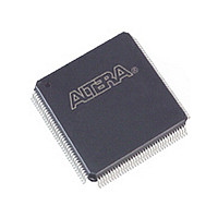
EPM1270GT144I5N Altera, EPM1270GT144I5N Datasheet - Page 15

EPM1270GT144I5N
Manufacturer Part Number
EPM1270GT144I5N
Description
MAX II
Manufacturer
Altera
Datasheet
1.EPM1270GT144I5N.pdf
(88 pages)
Specifications of EPM1270GT144I5N
Family Name
MAX II
Memory Type
Flash
# Macrocells
980
Frequency (max)
1.8797GHz
Propagation Delay Time
10ns
Number Of Logic Blocks/elements
127
# I/os (max)
116
Operating Supply Voltage (typ)
1.8V
In System Programmable
Yes
Operating Supply Voltage (min)
1.71V
Operating Supply Voltage (max)
1.89V
Operating Temp Range
-40C to 100C
Operating Temperature Classification
Industrial
Mounting
Surface Mount
Pin Count
144
Package Type
TQFP
Lead Free Status / Rohs Status
Compliant
Available stocks
Company
Part Number
Manufacturer
Quantity
Price
Company:
Part Number:
EPM1270GT144I5N
Manufacturer:
ALTERA
Quantity:
612
Chapter 2: MAX II Architecture
Logic Elements
Figure 2–6. MAX II LE
© October 2008 Altera Corporation
Reset (DEV_CLRn)
labpre/aload
labclkena1
labclkena2
Chip-Wide
labclk1
labclk2
labclr1
labclr2
data1
data2
data3
data4
addnsub
Each LE’s programmable register can be configured for D, T, JK, or SR operation. Each
register has data, true asynchronous load data, clock, clock enable, clear, and
asynchronous load/preset inputs. Global signals, general-purpose I/O pins, or any
LE can drive the register’s clock and clear control signals. Either general-purpose I/O
pins or LEs can drive the clock enable, preset, asynchronous load, and asynchronous
data. The asynchronous load data input comes from the data3 input of the LE. For
combinational functions, the LUT output bypasses the register and drives directly to
the LE outputs.
Each LE has three outputs that drive the local, row, and column routing resources. The
LUT or register output can drive these three outputs independently. Two LE outputs
drive column or row and DirectLink routing connections and one drives local
interconnect resources. This allows the LUT to drive one output while the register
drives another output. This register packing feature improves device utilization
because the device can use the register and the LUT for unrelated functions. Another
special packing mode allows the register output to feed back into the LUT of the same
LE so that the register is packed with its own fan-out LUT. This provides another
mechanism for improved fitting. The LE can also drive out registered and
unregistered versions of the LUT output.
Clock Enable
Asynchronous
Clear/Preset/
Load Logic
Clock and
LAB Carry-In
Select
Carry-In1
Carry-In0
Look-Up
Table
(LUT)
Chain
Carry
Register chain
routing from
previous LE
Carry-Out0
Carry-Out1
LAB Carry-Out
Synchronous
LAB-wide
Synchronous
Load
Clear Logic
Load and
Synchronous
LAB-wide
Clear
Register Bypass
Packed
Register Select
ADATA
D
ENA
PRN/ALD
CLRN
Register
Feedback
Q
Programmable
Register
MAX II Device Handbook
LUT chain
routing to next LE
Row, column,
and DirectLink
routing
Row, column,
and DirectLink
routing
Local routing
Register chain
output
2–7


