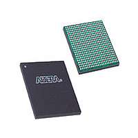
EP3C16F484I7N Altera, EP3C16F484I7N Datasheet - Page 73

EP3C16F484I7N
Manufacturer Part Number
EP3C16F484I7N
Description
Cyclone III
Manufacturer
Altera
Datasheet
1.EP3C16F484I7N.pdf
(274 pages)
Specifications of EP3C16F484I7N
Family Name
Cyclone III
Number Of Logic Blocks/elements
15408
# I/os (max)
346
Frequency (max)
437.5MHz
Process Technology
65nm
Operating Supply Voltage (typ)
1.2V
Logic Cells
15408
Ram Bits
516096
Operating Supply Voltage (min)
1.15V
Operating Supply Voltage (max)
1.25V
Operating Temp Range
-40C to 100C
Operating Temperature Classification
Industrial
Mounting
Surface Mount
Pin Count
484
Package Type
FBGA
Lead Free Status / Rohs Status
Compliant
Available stocks
Company
Part Number
Manufacturer
Quantity
Price
Company:
Part Number:
EP3C16F484I7N
Manufacturer:
ALTERA
Quantity:
4 000
Company:
Part Number:
EP3C16F484I7N
Manufacturer:
ALTERA41
Quantity:
60
Part Number:
EP3C16F484I7N
Manufacturer:
ALTERA/阿尔特拉
Quantity:
20 000
- Current page: 73 of 274
- Download datasheet (6Mb)
Chapter 5: Clock Networks and PLLs in the Cyclone III Device Family
PLLs in the Cyclone III Device Family
PLLs in the Cyclone III Device Family
© December 2009
f
Altera Corporation
Altera recommends using the clkena signals when switching the clock source to the
PLLs or the GCLK. The recommended sequence is:
1. Disable the primary output clock by deasserting the clkena signal.
2. Switch to the secondary clock using the dynamic select signals of the clock control
3. Allow some clock cycles of the secondary clock to pass before reasserting the
The Cyclone III device family offers up to four PLLs that provide robust clock
management and synthesis for device clock management, external system clock
management, and high-speed I/O interfaces.
For more information about the number of PLLs in each device density, refer to the
Cyclone III Device Family Overview
The Cyclone III device family PLLs have the same core analog structure.
Table 5–3
Table 5–3. Cyclone III Device Family PLL Hardware Features
C (output counters)
M, N, C counter sizes
Dedicated clock outputs
Clock input pins
Spread-spectrum input clock tracking
PLL cascading
Compensation modes
Phase shift resolution
Programmable duty cycle
Output counter cascading
Input clock switchover
User mode reconfiguration
Loss of lock detection
Notes to
(1) C counters range from 1 through 512 if the output clock uses a 50% duty cycle. For any output clocks using a
(2) Only applicable if the input clock jitter is in the input jitter tolerance specifications.
(3) The smallest phase shift is determined by the voltage-controlled oscillator (VCO) period divided by eight. For
block.
clkena signal. The exact number of clock cycles you must wait before enabling
the secondary clock is design-dependent. You can build custom logic to ensure
glitch-free transition when switching between different clock sources.
non-50% duty cycle, the post-scale counters range from 1 through 256.
degree increments, the Cyclone III device family can shift all output frequencies in increments of at least 45°.
Smaller degree increments are possible depending on the frequency and divide parameters.
Table
lists the features available in the Cyclone III device family PLLs.
5–3:
Hardware Features
chapter.
5
1 to 512
1 single-ended or 1 differential pair
4 single-ended or 2 differential pairs
Through GCLK
Source-Synchronous Mode, No Compensation
Mode, Normal Mode, and Zero Delay Buffer Mode
Down to 96-ps increments
(1)
Cyclone III Device Handbook, Volume 1
Availability
v
v
v
v
v
v
(2)
(3)
5–9
Related parts for EP3C16F484I7N
Image
Part Number
Description
Manufacturer
Datasheet
Request
R

Part Number:
Description:
CYCLONE II STARTER KIT EP2C20N
Manufacturer:
Altera
Datasheet:

Part Number:
Description:
CPLD, EP610 Family, ECMOS Process, 300 Gates, 16 Macro Cells, 16 Reg., 16 User I/Os, 5V Supply, 35 Speed Grade, 24DIP
Manufacturer:
Altera Corporation
Datasheet:

Part Number:
Description:
CPLD, EP610 Family, ECMOS Process, 300 Gates, 16 Macro Cells, 16 Reg., 16 User I/Os, 5V Supply, 15 Speed Grade, 24DIP
Manufacturer:
Altera Corporation
Datasheet:

Part Number:
Description:
Manufacturer:
Altera Corporation
Datasheet:

Part Number:
Description:
CPLD, EP610 Family, ECMOS Process, 300 Gates, 16 Macro Cells, 16 Reg., 16 User I/Os, 5V Supply, 30 Speed Grade, 24DIP
Manufacturer:
Altera Corporation
Datasheet:

Part Number:
Description:
High-performance, low-power erasable programmable logic devices with 8 macrocells, 10ns
Manufacturer:
Altera Corporation
Datasheet:

Part Number:
Description:
High-performance, low-power erasable programmable logic devices with 8 macrocells, 7ns
Manufacturer:
Altera Corporation
Datasheet:

Part Number:
Description:
Classic EPLD
Manufacturer:
Altera Corporation
Datasheet:

Part Number:
Description:
High-performance, low-power erasable programmable logic devices with 8 macrocells, 10ns
Manufacturer:
Altera Corporation
Datasheet:

Part Number:
Description:
Manufacturer:
Altera Corporation
Datasheet:

Part Number:
Description:
Manufacturer:
Altera Corporation
Datasheet:

Part Number:
Description:
Manufacturer:
Altera Corporation
Datasheet:

Part Number:
Description:
CPLD, EP610 Family, ECMOS Process, 300 Gates, 16 Macro Cells, 16 Reg., 16 User I/Os, 5V Supply, 25 Speed Grade, 24DIP
Manufacturer:
Altera Corporation
Datasheet:


