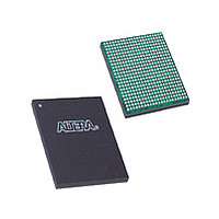
EP3C16F484I7N Altera, EP3C16F484I7N Datasheet - Page 132

EP3C16F484I7N
Manufacturer Part Number
EP3C16F484I7N
Description
Cyclone III
Manufacturer
Altera
Datasheet
1.EP3C16F484I7N.pdf
(274 pages)
Specifications of EP3C16F484I7N
Family Name
Cyclone III
Number Of Logic Blocks/elements
15408
# I/os (max)
346
Frequency (max)
437.5MHz
Process Technology
65nm
Operating Supply Voltage (typ)
1.2V
Logic Cells
15408
Ram Bits
516096
Operating Supply Voltage (min)
1.15V
Operating Supply Voltage (max)
1.25V
Operating Temp Range
-40C to 100C
Operating Temperature Classification
Industrial
Mounting
Surface Mount
Pin Count
484
Package Type
FBGA
Lead Free Status / Rohs Status
Compliant
Available stocks
Company
Part Number
Manufacturer
Quantity
Price
Company:
Part Number:
EP3C16F484I7N
Manufacturer:
ALTERA
Quantity:
4 000
Company:
Part Number:
EP3C16F484I7N
Manufacturer:
ALTERA41
Quantity:
60
Part Number:
EP3C16F484I7N
Manufacturer:
ALTERA/阿尔特拉
Quantity:
20 000
- Current page: 132 of 274
- Download datasheet (6Mb)
7–8
Figure 7–2. Cyclone III Device Family LVDS Interface with True Output Buffer on the Left and Right I/O Banks
Figure 7–3. LVDS Interface with External Resistor Network on the Top and Bottom I/O Banks
Note to
(1)
BLVDS I/O Standard Support in the Cyclone III Device Family
Cyclone III Device Handbook, Volume 1
R
S
Transmitting Device
Figure
= 120
Ω;
7–3:
R
P
= 170
Cyclone III Device Family
txout -
txout +
Ω
LVDS Transmitter
Designing with LVDS
Cyclone III device family I/O banks support LVDS I/O standard. The left and right
I/O banks support true LVDS transmitters. On the top and bottom I/O banks, the
emulated LVDS transmitters are supported using two single-ended output buffers
with external resistors. One of the single-ended output buffers is programmed to have
opposite polarity. The LVDS receiver requires an external 100-Ω termination resistor
between the two signals at the input buffer.
Figure 7–2
LVDS output and input buffers.
Figure 7–3
LVDS using two single-ended output buffers and external resistors.
The BLVDS I/O standard is a high-speed differential data transmission technology
that extends the benefits of standard point-to-point LVDS to multipoint configuration
that supports bidirectional half-duplex communication. BLVDS differs from standard
LVDS by providing a higher drive to achieve similar signal swings at the receiver
while loaded with two terminations at both ends of the bus.
Emulated
50 Ω
50 Ω
100 Ω
rxin +
rxin -
shows a point-to-point LVDS interface using Cyclone III device family true
shows a point-to-point LVDS interface with Cyclone III device family
Input Buffer
Resistor Network
R S
R S
Cyclone III Device Family
R P
Family Logic
Cyclone III
Chapter 7: High-Speed Differential Interfaces in the Cyclone III Device Family
Device
Array
Output Buffer
50 Ω
50 Ω
100 Ω
txout +
txout -
50 Ω
50 Ω
LVDS Receiver
© December 2009 Altera Corporation
rxin +
rxin -
High-Speed I/O Standards Support
(Note 1)
100 Ω
Receiving Device
Related parts for EP3C16F484I7N
Image
Part Number
Description
Manufacturer
Datasheet
Request
R

Part Number:
Description:
CYCLONE II STARTER KIT EP2C20N
Manufacturer:
Altera
Datasheet:

Part Number:
Description:
CPLD, EP610 Family, ECMOS Process, 300 Gates, 16 Macro Cells, 16 Reg., 16 User I/Os, 5V Supply, 35 Speed Grade, 24DIP
Manufacturer:
Altera Corporation
Datasheet:

Part Number:
Description:
CPLD, EP610 Family, ECMOS Process, 300 Gates, 16 Macro Cells, 16 Reg., 16 User I/Os, 5V Supply, 15 Speed Grade, 24DIP
Manufacturer:
Altera Corporation
Datasheet:

Part Number:
Description:
Manufacturer:
Altera Corporation
Datasheet:

Part Number:
Description:
CPLD, EP610 Family, ECMOS Process, 300 Gates, 16 Macro Cells, 16 Reg., 16 User I/Os, 5V Supply, 30 Speed Grade, 24DIP
Manufacturer:
Altera Corporation
Datasheet:

Part Number:
Description:
High-performance, low-power erasable programmable logic devices with 8 macrocells, 10ns
Manufacturer:
Altera Corporation
Datasheet:

Part Number:
Description:
High-performance, low-power erasable programmable logic devices with 8 macrocells, 7ns
Manufacturer:
Altera Corporation
Datasheet:

Part Number:
Description:
Classic EPLD
Manufacturer:
Altera Corporation
Datasheet:

Part Number:
Description:
High-performance, low-power erasable programmable logic devices with 8 macrocells, 10ns
Manufacturer:
Altera Corporation
Datasheet:

Part Number:
Description:
Manufacturer:
Altera Corporation
Datasheet:

Part Number:
Description:
Manufacturer:
Altera Corporation
Datasheet:

Part Number:
Description:
Manufacturer:
Altera Corporation
Datasheet:

Part Number:
Description:
CPLD, EP610 Family, ECMOS Process, 300 Gates, 16 Macro Cells, 16 Reg., 16 User I/Os, 5V Supply, 25 Speed Grade, 24DIP
Manufacturer:
Altera Corporation
Datasheet:


