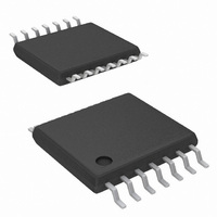
DG636EQ-T1-E3 Vishay, DG636EQ-T1-E3 Datasheet - Page 2

DG636EQ-T1-E3
Manufacturer Part Number
DG636EQ-T1-E3
Description
0.5pC Charge Injection, Dual SPDT AS
Manufacturer
Vishay
Datasheet
1.DG636EQ-T1-E3.pdf
(11 pages)
Specifications of DG636EQ-T1-E3
Function
Switch
Circuit
2 x SPDT
On-state Resistance
160 Ohm
Current - Supply
1µA
Operating Temperature
-40°C ~ 125°C
Mounting Type
Surface Mount
Package / Case
14-TSSOP
Number Of Switches
Dual
Switch Configuration
SPDT
On Resistance (max)
245 Ohm @ 3 V
On Time (max)
108 ns @ 3 V
Off Time (max)
76 ns @ 3 V
Off Isolation (typ)
- 58 dB
Bandwidth
610 MHz
Supply Voltage (max)
12 V
Supply Voltage (min)
2.7 V
Maximum Power Dissipation
450 mW
Maximum Operating Temperature
+ 125 C
Mounting Style
SMD/SMT
Minimum Operating Temperature
- 40 C
Switch Current (typ)
0.000001 mA/- 0.000001 mA @ +/- 5 V
Lead Free Status / RoHS Status
Lead free / RoHS Compliant
Lead Free Status / RoHS Status
Lead free / RoHS Compliant
Other names
DG636EQ-T1-E3TR
Available stocks
Company
Part Number
Manufacturer
Quantity
Price
Company:
Part Number:
DG636EQ-T1-E3
Manufacturer:
Cypress
Quantity:
96
DG636
Vishay Siliconix
Notes:
a. - 40 °C to 85 °C datasheet limits apply.
Notes:
a. Signals on SX, DX, or INX exceeding V+ or V- will be clamped by internal diodes. Limit forward diode current to maximum current ratings.
b. All leads welded or soldered to PC board.
c. Derate 5.6 mW/°C above 70 °C.
d. Derate 6.6 mW/°C above 70 °C.
e. Manual soldering with iron is not recommended for leadless components. The miniQFN-16 is a leadless package. The end of the lead terminal
www.vishay.com
2
TRUTH TABLE
ORDERING INFORMATION
ABSOLUTE MAXIMUM RATINGS (T
Parameter
V+ to V-
GND to V-
Digital Inputs
Continuous Current (Any Terminal)
Peak Current, S or D (Pulsed 1 ms, 10 % Duty Cycle)
Storage Temperature
Power Dissipation (Package)
Thermal Resistance (Package)
SPECIFICATIONS FOR DUAL SUPPLIES
Parameter
Analog Switch
Analog Signal Range
On-Resistance
On-Resistance Match
On-Resistance Flatness
is exposed copper (not plated) as a result of the singulation process in manufacturing. A solder fillet at the exposed copper lip cannot be
guaranteed and is not required to ensure adequate bottom side solder interconnection.
- 40 °C to 125 °C
Temp. Range
Enable
Input
H
H
H
H
L
a
, V
S
, V
D
e
a
R
V
Symbol
FLATNESS
R
b
ANALOG
R
DS(on)
b
ON
A1
X
H
H
L
L
V
IN A0, A1 and ENABLE
I
I
Selected Input
S
S
Unless Otherwise Specified
= 1 mA, V
= 1 mA, V
I
16 pin miniQFN
S
14 pin TSSOP
V+ = 5 V, V- = - 5 V
Test Conditions
= 1 mA, V
14 pin TSSOP
16 pin miniQFN
14 pin TSSOP
16 pin miniQFN
Package
A
D
D
= 25 °C, unless otherwise noted)
= - 3 V, 0 V, + 3 V
= - 3 V, 0 V, + 3 V
D
A0
H
H
X
= 2.0 V, 0.8 V
L
L
= ± 3 V
c
d, e
a
Temp.
Room
Room
Room
Full
Full
Full
Full
b
or 30 mA, whichever occurs first
Typ.
70
10
1
(V-) - 0.3 to (V+) + 0.3
c
D1 to S1A, D2 to S2A
D1 to S1B, D2 to S2A
D1 to S1A, D2 to S2B
D1 to S1B, D2 to S2B
- 65 to 150
- 40 °C to 125 °C - 40 °C to 85 °C
All Switches Open
Min.
Limit
- 5
DG636EQ-T1-E3
On Switches
DG636EN-T1-E4
100
450
525
178
152
14
30
7
Part Number
d
DG636
Max.
115
160
6.5
20
33
5
5
S10-1815-Rev. D, 02-Aug-10
d
Document Number: 69901
Min.
- 5
d
Max.
115
140
6.5
20
22
5
5
°C/W
d
Unit
mW
mA
°C
V
Unit
V


