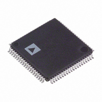
ADV7183BBSTZ Analog Devices Inc, ADV7183BBSTZ Datasheet - Page 8

ADV7183BBSTZ
Manufacturer Part Number
ADV7183BBSTZ
Description
IC,TV/VIDEO CIRCUIT,Color Decoder Circuit,CMOS,QFP,80PIN,PLASTIC
Manufacturer
Analog Devices Inc
Type
Video Decoderr
Datasheet
1.ADV7183BKSTZ.pdf
(100 pages)
Specifications of ADV7183BBSTZ
Applications
Projectors, Recorders, Security
Voltage - Supply, Analog
3.15 V ~ 3.45 V
Voltage - Supply, Digital
1.65 V ~ 2 V
Mounting Type
Surface Mount
Package / Case
80-LQFP
Lead Free Status / RoHS Status
Lead free / RoHS Compliant
Available stocks
Company
Part Number
Manufacturer
Quantity
Price
Company:
Part Number:
ADV7183BBSTZ
Manufacturer:
AD
Quantity:
670
Company:
Part Number:
ADV7183BBSTZ
Manufacturer:
Analog Devices Inc
Quantity:
10 000
ADV7183B
TIMING SPECIFICATIONS
Guaranteed by characterization. At A
operating temperature range, unless otherwise specified.
Table 3.
Parameter
SYSTEM CLOCK AND CRYSTAL
I
RESET FEATURE
CLOCK OUTPUTS
DATA AND CONTROL OUTPUTS
1
2
ANALOG SPECIFICATIONS
Guaranteed by characterization. A
temperature range, unless otherwise noted). Recommended analog input video signal range: 0.5 V to 1.6 V, typically 1 V p-p.
Table 4.
Parameter
CLAMP CIRCUITRY
1
2
2
Temperature range: T
The min/max specifications are guaranteed over this range.
Temperature range: T
The min/max specifications are guaranteed over this range.
C PORT
Nominal Frequency
Frequency Stability
SCLK Frequency
SCLK Min Pulse Width High
SCLK Min Pulse Width Low
Hold Time (Start Condition)
Setup Time (Start Condition)
SDA Setup Time
SCLK and SDA Rise Time
SCLK and SDA Fall Time
Setup Time for Stop Condition
Reset Pulse Width
LLC1 Mark Space Ratio
LLC1 Rising to LLC2 Rising
LLC1 Rising to LLC2 Falling
Data Output Transitional Time
Data Output Transitional Time
Propagation Delay to Hi-Z
Max Output Enable Access Time
Min Output Enable Access Time
External Clamp Capacitor
Input Impedance
Large Clamp Source Current
Large Clamp Sink Current
Fine Clamp Source Current
Fine Clamp Sink Current
9 F
1 1 F
1,
1,
1 0 F
1 2 F
2
2
MIN
MIN
to T
to T
MAX
MAX
, –40°C to +85°C (0°C to 70°C for ADV7183BKSTZ).
, –40°C to +85°C (0°C to 70°C for ADV7183BKSTZ).
VDD
VDD
= 3.15 V to 3.45 V, D
= 3.15 V to 3.45 V, D
Symbol
t
t
t
t
t
t
t
t
t
t
t
t
t
t
t
t
1
2
3
4
5
6
7
8
9
11
12
13
14
15
16
17
:t
Symbol
10
VDD
Test Conditions
Negative clock edge to start of
valid data; (t
End of valid data to negative clock
edge; (t
Rev. B | Page 8 of 100
VDD
= 1.65 V to 2.0 V, D
Test Conditions
Clamps switched off
= 1.65 V to 2.0 V, D
HOLD
= t
ACCESS
9
+ t
= t
14
)
10
– t
VDDIO
13
VDDIO
)
= 3.0 V to 3.6 V, P
= 3.0 V to 3.6 V, P
Min
0.6
1.3
0.6
0.6
100
5
45:55
Min
VDD
Typ
28.6363
0.6
0.5
0.5
6
7
4
Typ
0.1
10
0.75
0.75
60
60
VDD
= 1.65 V to 2.0 V (operating
= 1.65 V to 2.0 V,
Max
±50
400
300
300
55:45
3.4
2.4
Max
Unit
kHz
MHz
ppm
μs
μs
μs
μs
ns
ns
ns
μs
ms
% duty cycle
ns
ns
ns
ns
ns
ns
ns
Unit
μF
MΩ
mA
mA
μA
μA


