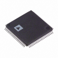
ADV7183BBSTZ Analog Devices Inc, ADV7183BBSTZ Datasheet - Page 17

ADV7183BBSTZ
Manufacturer Part Number
ADV7183BBSTZ
Description
IC,TV/VIDEO CIRCUIT,Color Decoder Circuit,CMOS,QFP,80PIN,PLASTIC
Manufacturer
Analog Devices Inc
Type
Video Decoderr
Datasheet
1.ADV7183BKSTZ.pdf
(100 pages)
Specifications of ADV7183BBSTZ
Applications
Projectors, Recorders, Security
Voltage - Supply, Analog
3.15 V ~ 3.45 V
Voltage - Supply, Digital
1.65 V ~ 2 V
Mounting Type
Surface Mount
Package / Case
80-LQFP
Lead Free Status / RoHS Status
Lead free / RoHS Compliant
Available stocks
Company
Part Number
Manufacturer
Quantity
Price
Company:
Part Number:
ADV7183BBSTZ
Manufacturer:
AD
Quantity:
670
Company:
Part Number:
ADV7183BBSTZ
Manufacturer:
Analog Devices Inc
Quantity:
10 000
GLOBAL PIN CONTROL
Three-State Output Drivers
TOD, Address 0x03[6]
This bit allows the user to three-state the output drivers of the
ADV7183B.
Upon setting the TOD bit, the P15 to P0, HS, VS, FIELD, and
SFL pins are three-stated.
The timing pins (HS/VS/FIELD) can be forced active via the
TIM_OE bit. For more information on three-state control, refer
to the
Enable sections.
Individual drive strength controls are provided via the
DR_STR_XX bits.
The ADV7183B supports three-stating via a dedicated pin.
When set high, the OE pin three-states the output drivers for
the P15 to P0, HS, VS, FIELD, and SFL pins. The output drivers
are three-stated if the TOD bit or the OE pin is set high.
When TOD is 0 (default), the output drivers are enabled.
When TOD is 1, the output drivers are three-stated.
Three-State LLC Driver
TRI_LLC, Address 0x1D[7]
This bit allows the output drivers for the LLC1 and LLC2 pins
of the ADV7183B to be three-stated. For more information on
three-state control, refer to the
the
Individual drive strength controls are provided via the
DR_STR_XX bits.
When TRI_LLC is 0 (default), the LLC pin drivers work
according to the DR_STR_C[1:0] setting (pin enabled).
When TRI_LLC is 1, the LLC pin drivers are three-stated.
1 5 2 H
T iming Signals Output Enable sections.
T hree-State LLC Driver and the
1 4 9 H
T hree-State Output Drivers and
1 5 1 H
T iming Signals Output
1 5 0 H
Rev. B | Page 17 of 100
Timing Signals Output Enable
TIM_OE, Address 0x04[3]
The TIM_OE bit should be regarded as an addition to the TOD
bit. Setting it high forces the output drivers for HS, VS, and
FIELD pins into the active (driving) state even if the TOD bit is
set. If set to low, the HS, VS, and FIELD pins are three-stated,
dependent on the TOD bit. This functionality is useful if the
decoder is used as a timing generator only. This can happen
when only the timing signals are to be extracted from an
incoming signal, or if the part is in free-run mode where a
separate chip can output, for an example, a company logo.
For more information on three-state control, refer to the
State Output Drivers and the
Individual drive strength controls are provided via the
DR_STR_XX bits.
When TIM_OE is 0 (default), the HS, VS, and FIELD pins are
three-stated according to the TOD bit.
When TIM_OE is 1, HS, VS, and FIELD are forced active all
the time.
Drive Strength Selection (Data)
DR_STR[1:0] Address 0xF4[5:4]
For EMC and crosstalk reasons, it can be desirable to strengthen
or weaken the drive strength of the output drivers. The
DR_STR[1:0] bits affect the P[15:0] output drivers.
For more information on three-state control, refer to the
Strength Selection (Clock) and the
(Sync) sections.
Table 11. DR_STR Function
DR_STR[1:0]
00
01 (default)
10
11
Description
Low drive strength (1×)
Medium low drive strength (2×)
Medium high drive strength (3×)
High drive strength (4×)
T hree-State LLC Driver sections.
1 5 4 H
1 5 6 H
D rive Strength Selection
ADV7183B
T hree-
1 5 3 H
D rive
1 5 5 H


