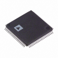
ADV7183BBSTZ Analog Devices Inc, ADV7183BBSTZ Datasheet - Page 6

ADV7183BBSTZ
Manufacturer Part Number
ADV7183BBSTZ
Description
IC,TV/VIDEO CIRCUIT,Color Decoder Circuit,CMOS,QFP,80PIN,PLASTIC
Manufacturer
Analog Devices Inc
Type
Video Decoderr
Datasheet
1.ADV7183BKSTZ.pdf
(100 pages)
Specifications of ADV7183BBSTZ
Applications
Projectors, Recorders, Security
Voltage - Supply, Analog
3.15 V ~ 3.45 V
Voltage - Supply, Digital
1.65 V ~ 2 V
Mounting Type
Surface Mount
Package / Case
80-LQFP
Lead Free Status / RoHS Status
Lead free / RoHS Compliant
Available stocks
Company
Part Number
Manufacturer
Quantity
Price
Company:
Part Number:
ADV7183BBSTZ
Manufacturer:
AD
Quantity:
670
Company:
Part Number:
ADV7183BBSTZ
Manufacturer:
Analog Devices Inc
Quantity:
10 000
ADV7183B
SPECIFICATIONS
ELECTRICAL CHARACTERISTICS
At A
otherwise specified.
Table 1.
Parameter
STATIC PERFORMANCE
DIGITAL INPUTS
DIGITAL OUTPUTS
POWER REQUIREMENTS
1
2
3
4
5
6
7
Temperature range: T
The min/max specifications are guaranteed over this range.
Pins 36 and 79.
Pins 1, 2, 5, 6, 8, 12, 17, 18 to 24, 32 to 35, 74 to 76, 80.
Guaranteed by characterization.
ADC1 powered on.
All three ADCs powered on.
Resolution (each ADC)
Integral Nonlinearity
Differential Nonlinearity
Input High Voltage
Input Low Voltage
Input Current
Input Capacitance
Output High Voltage
Output Low Voltage
High Impedance Leakage Current
Output Capacitance
Digital Core Power Supply
Digital I/O Power Supply
PLL Power Supply
Analog Power Supply
Digital Core Supply Current
Digital I/O Supply Current
PLL Supply Current
Analog Supply Current
Power-Down Current
Power-Up Time
VDD
= 3.15 V to 3.45 V, D
0 F
1,
1 F
2
MIN
to T
4 F
5
MAX
, –40°C to +85°C (0°C to 70°C for ADV7183BKSTZ).
VDD
= 1.65 V to 2.0 V, D
Symbol
N
DNL
V
V
I
C
V
V
I
C
D
D
P
A
I
I
I
I
I
t
INL
IN
LEAK
DVDD
DVDDIO
PVDD
AVDD
PWRDN
PWRUP
IH
IL
IN
OH
OL
OUT
VDD
VDD
VDD
VDDIO
VDDIO
= 3.0 V to 3.6 V, P
Rev. B | Page 6 of 100
Test Conditions
BSL at 54 MHz
BSL at 54 MHz
Pins listed in Note
All other pins
I
I
Pins listed in Note
All other pins
CVBS input
YPrPb input
SOURCE
SINK
= 3.2 mA
= 0.4 mA
5 F
6
6 F
7
VDD
= 1.65 V to 2.0 V, operating temperature range, unless
2 F
3 F
3
4
Min
2
–50
–10
2.4
1.65
3.0
1.65
3.15
Typ
–0.475/+0.6
–0.25/+0.5
1.8
3.3
1.8
3.3
82
2
10.5
85
180
1.5
20
Max
10
±3
–0.7/+2
0.8
+50
+10
10
0.4
50
10
20
2
3.6
2.0
3.45
Unit
Bits
V
μA
μA
pF
V
μA
μA
pF
mA
mA
mA
mA
mA
mA
ms
LSB
LSB
V
V
V
V
V
V


