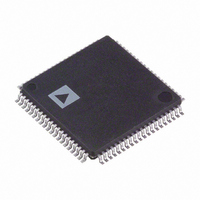
ADV7183BBSTZ Analog Devices Inc, ADV7183BBSTZ Datasheet - Page 46

ADV7183BBSTZ
Manufacturer Part Number
ADV7183BBSTZ
Description
IC,TV/VIDEO CIRCUIT,Color Decoder Circuit,CMOS,QFP,80PIN,PLASTIC
Manufacturer
Analog Devices Inc
Type
Video Decoderr
Datasheet
1.ADV7183BKSTZ.pdf
(100 pages)
Specifications of ADV7183BBSTZ
Applications
Projectors, Recorders, Security
Voltage - Supply, Analog
3.15 V ~ 3.45 V
Voltage - Supply, Digital
1.65 V ~ 2 V
Mounting Type
Surface Mount
Package / Case
80-LQFP
Lead Free Status / RoHS Status
Lead free / RoHS Compliant
Available stocks
Company
Part Number
Manufacturer
Quantity
Price
Company:
Part Number:
ADV7183BBSTZ
Manufacturer:
AD
Quantity:
670
Company:
Part Number:
ADV7183BBSTZ
Manufacturer:
Analog Devices Inc
Quantity:
10 000
ADV7183B
PVENDSIGN PAL Vsync End Sign, Address 0xE9[5]
Setting PVENDSIGN to 0 (default) delays the end of Vsync. Set
for user manual programming.
Setting PVENDSIGN to 1 advances the end of Vsync. Not
recommended for user programming.
PVEND[4:0] PAL Vsync End, Address 0xE9[4:0]
The default value of PVEND is 10100, indicating the PAL Vsync
end position.
For all NTSC/PAL Vsync timing controls, both the V bit in the
AV code and the Vsync on the VS pin are modified.
PFTOGDELO PAL Field Toggle Delay on Odd Field,
Address 0xEA[7]
When PFTOGDELO is 0 (default), there is no delay.
Setting PFTOGDELO to 1 delays the F toggle/transition on an
odd field by a line relative to PFTOG.
PFTOGDELE PAL Field Toggle Delay on Even Field,
Address 0xEA[6]
When PFTOGDELE is 0, there is no delay.
Setting PFTOGDELE to 1 (default) delays the F toggle/
transition on an even field by a line relative to PFTOG.
PFTOGSIGN PAL Field Toggle Sign, Address 0xEA[5]
Setting PFTOGSIGN to 0 delays the field transition. Set for user
manual programming.
Setting PFTOGSIGN to 1 (default) advances the field transition.
Not recommended for user programming.
PFTOG PAL Field Toggle, Address 0xEA[4:0]
The default value of PFTOG is 00011, indicating the PAL field
toggle position.
For all NTSC/PAL Field timing controls, the F bit in the AV
code and the field signal on the FIELD/DE pin are modified.
Rev. B | Page 46 of 100
SYNC PROCESSING
The ADV7183B has two additional sync processing blocks that
postprocess the raw synchronization information extracted
from the digitized input video. If desired, the blocks can be
disabled via the following two I
ENHSPLL Enable Hsync Processor, Address 0x01[6]
The Hsync processor is designed to filter incoming Hsyncs that
have been corrupted by noise, providing improved performance
for video signals with stable time bases but poor SNR.
Setting ENHSPLL to 0 disables the Hsync processor.
Setting ENHSPLL to 1 (default) enables the Hsync processor.
ENVSPROC Enable Vsync Processor, Address 0x01[3]
This block provides extra filtering of the detected Vsyncs to give
improved vertical lock.
Setting ENVSPROC to 0 disables the Vsync processor.
Setting ENVSPROC to 1 (default) enables the Vsync processor.
NOT VALID FOR USER
PROGRAMMING
ADVANCE TOGGLE OF
FIELD BY PTOG[4:0]
PFTOGDELO
ADDITIONAL
DELAY BY
1 LINE
YES
1
Figure 30. PAL F Toggle
1
0
PFTOGSIGN
ODD FIELD?
TOGGLE
2
FIELD
C bits.
0
FIELD BY PFTOG[4:0]
DELAY TOGGLE OF
PFTOGDELE
ADDITIONAL
DELAY BY
0
1 LINE
NO
1


