ADUC7122BBCZ-RL Analog Devices Inc, ADUC7122BBCZ-RL Datasheet - Page 4
ADUC7122BBCZ-RL
Manufacturer Part Number
ADUC7122BBCZ-RL
Description
PRECISION ANALOG MCU I.C
Manufacturer
Analog Devices Inc
Series
MicroConverter® ADuC7xxxr
Datasheet
1.ADUC7122BBCZ.pdf
(96 pages)
Specifications of ADUC7122BBCZ-RL
Core Processor
ARM7
Core Size
16/32-Bit
Speed
41.78MHz
Connectivity
I²C, SPI, UART/USART
Peripherals
POR, PWM, WDT
Number Of I /o
32
Program Memory Size
126KB (63K x 16)
Program Memory Type
FLASH
Ram Size
8K x 8
Voltage - Supply (vcc/vdd)
3 V ~ 3.6 V
Data Converters
A/D 13x12b, D/A 12x12b
Oscillator Type
Internal
Operating Temperature
-10°C ~ 95°C
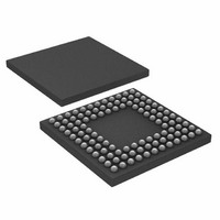
Package / Case
108-LFBGA, CSPBGA
Lead Free Status / RoHS Status
Lead free / RoHS Compliant
Eeprom Size
-
Lead Free Status / RoHS Status
Lead free / RoHS Compliant
Other names
ADUC7122BBCZ-RL
ADUC7122BBCZ-RLTR
ADUC7122BBCZ-RLTR
Available stocks
Company
Part Number
Manufacturer
Quantity
Price
Company:

Part Number:
ADUC7122BBCZ-RL
Manufacturer:
Analog Devices Inc
Quantity:
10 000


ADuC7122
GENERAL DESCRIPTION
The ADuC7122 is a fully integrated, 1 MSPS, 12-bit data acquisi-
tion system, incorporating high performance multichannel
ADCs, 12 voltage output DACs, 16-bit/32-bit MCUs, and
Flash/EE memory on a single chip.
The ADC consists of up to 13 inputs. Four of these inputs can
be configured as differential pairs with a programmable gain
amplifier on their front end, providing a gain between 1 and 5.
The ADC can operate in single-ended or differential input
mode. The ADC input voltage is 0 V to V
gap reference, temperature sensor, and supply voltage monitor
complete the ADC peripheral set.
The DAC output range is programmable to one of two voltage
ranges. The DAC outputs have an enhanced feature of being
able to retain their output voltage during a watchdog or
software reset sequence.
The device operates from an on-chip oscillator and a PLL,
generating an internal high frequency clock of 41.78 MHz. This
clock is routed through a programmable clock divider from
which the MCU core clock operating frequency is generated.
The microcontroller core is an ARM7TDMI®, 16-bit/32-bit
RISC machine that offers up to 41 MIPS peak performance.
There are 8 kB of SRAM and 126 kB of nonvolatile Flash/EE
REF
. A low drift band
Rev. 0 | Page 4 of 96
memory provided on chip. The ARM7TDMI core views all
memory and registers as a single linear array.
The ADuC7122 contains an advanced interrupt controller. The
vectored interrupt controller (VIC) allows every interrupt to be
assigned a priority level. It also supports nested interrupts to a
maximum level of eight per IRQ and FIQ. When IRQ and FIQ
interrupt sources are combined, a total of 16 nested interrupt
levels are supported.
On-chip factory firmware supports in-circuit download via the
I
supported via the JTAG interface. These features are incorporated
into a low cost QuickStart™ development system supporting this
MicroConverter® family. The part contains a 16-bit PWM with
six output signals.
For communication purposes, the part contains 2× I
that can be individually configured for master or slave mode.
An SPI interface supporting both master and slave modes is
also provided.
The part operates from 3.0 V to 3.6 V and is specified over a
temperature range of −10°C to +95°C. The ADuC7122 is
available in a 108-ball BGA package.
2
C serial interface port, and nonintrusive emulation is also
2
C channels
Related parts for ADUC7122BBCZ-RL
Image
Part Number
Description
Manufacturer
Datasheet
Request
R

Part Number:
Description:
±1.7g Dual-Axis IMEMS Accelerometer Evaluation Board
Manufacturer:
Analog Devices Inc
Datasheet:

Part Number:
Description:
Inertial Sensor Evaluation System
Manufacturer:
Analog Devices Inc
Datasheet:
Part Number:
Description:
Manufacturer:
Analog Devices Inc
Datasheet:
Part Number:
Description:
Manufacturer:
Analog Devices Inc
Datasheet:
Part Number:
Description:
Manufacturer:
Analog Devices Inc
Datasheet:
Part Number:
Description:
Manufacturer:
Analog Devices Inc
Datasheet:
Part Number:
Description:
Manufacturer:
Analog Devices Inc
Datasheet:
Part Number:
Description:
Manufacturer:
Analog Devices Inc
Datasheet:
Part Number:
Description:
Manufacturer:
Analog Devices Inc
Datasheet:
Part Number:
Description:
Manufacturer:
Analog Devices Inc
Datasheet:
Part Number:
Description:
Manufacturer:
Analog Devices Inc
Datasheet:
Part Number:
Description:
Manufacturer:
Analog Devices Inc
Datasheet:
Part Number:
Description:
Manufacturer:
Analog Devices Inc
Datasheet: