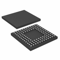
ADUC7122BBCZ-RL Analog Devices Inc, ADUC7122BBCZ-RL Datasheet - Page 29

ADUC7122BBCZ-RL
Manufacturer Part Number
ADUC7122BBCZ-RL
Description
PRECISION ANALOG MCU I.C
Manufacturer
Analog Devices Inc
Series
MicroConverter® ADuC7xxxr
Datasheet
1.ADUC7122BBCZ.pdf
(96 pages)
Specifications of ADUC7122BBCZ-RL
Core Processor
ARM7
Core Size
16/32-Bit
Speed
41.78MHz
Connectivity
I²C, SPI, UART/USART
Peripherals
POR, PWM, WDT
Number Of I /o
32
Program Memory Size
126KB (63K x 16)
Program Memory Type
FLASH
Ram Size
8K x 8
Voltage - Supply (vcc/vdd)
3 V ~ 3.6 V
Data Converters
A/D 13x12b, D/A 12x12b
Oscillator Type
Internal
Operating Temperature
-10°C ~ 95°C
Package / Case
108-LFBGA, CSPBGA
Lead Free Status / RoHS Status
Lead free / RoHS Compliant
Eeprom Size
-
Lead Free Status / RoHS Status
Lead free / RoHS Compliant
Other names
ADUC7122BBCZ-RL
ADUC7122BBCZ-RLTR
ADUC7122BBCZ-RLTR
Available stocks
Company
Part Number
Manufacturer
Quantity
Price
Company:
Part Number:
ADUC7122BBCZ-RL
Manufacturer:
Analog Devices Inc
Quantity:
10 000
All the controls are independently set through register bits to
give maximum flexibility to the user. Typically, users must set
the following:
1.
2.
3.
TYPICAL OPERATION
Once configured via the ADC control and channel selection
registers, the ADC converts the analog input and provides a
12-bit result in the ADCDAT register.
The top four bits are the sign bits, and the 12-bit result is placed
from Bit 16 to Bit 27, as shown in Figure 15. Note that in fully
differential mode, the result is represented in twos complement
format, and in pseudo differential and single-ended mode, the
result is represented in straight binary format.
Calibration
By default, the factory-set values written to the ADC offset
(ADCOF) and gain coefficient registers (ADCGN) yield opti-
mum performance in terms of end-point errors and linearity for
standalone operation of the part (see the General Description
section). If system calibration is required, it is possible to mod-
ify the default offset and gain coefficients to improve end-point
errors, but note that any modification to the factory-set ADCOF
and ADCGN values can degrade ADC linearity performance.
For system offset error correction, the ADC channel input stage
must be tied to AGND. A continuous software ADC conversion
loop must be implemented by modifying the value in ADCOF
until the ADC result (ADCDAT) reads Code 0 to Code 1. If
the ADCDAT value is greater than 1, ADCOF should be decre-
mented until ADCDAT reads Code 0 to Code 1. Offset error
correction is performed digitally and has a resolution of 0.25 LSB
and a range of ±3.125% of V
For system gain error correction, the ADC channel input stage
must be tied to V
loop must be implemented to modify the value in ADCGN
until ADCDAT reads Code 4094 to Code 4095. If the ADCDAT
value is less than 4094, ADCGN should be incremented until
ADCDAT reads Code 4094 to Code 4095. Similar to the offset
calibration, the gain calibration resolution is 0.25 LSB with a
range of ±3% of V
31
SIGN BITS
Select PADCxP as the PGA input. Enable the PADCxN
buffer and optionally disable the PADCxP input buffer.
Set the proper gain value for the PGA. Bypass the
PADCxN buffer if a grounded signal is required.
Set the ADC to pseudo differential mode and start the
conversion.
27
REF
REF
Figure 15. ADC Result Format
. A continuous software ADC conversion
.
12-BIT ADC RESULT
REF
.
16 15
0
Rev. 0 | Page 29 of 96
Current Consumption
The ADC in standby mode, that is, powered up but not
converting, typically consumes 640 μA. The internal reference
adds 140 μA. During conversion, the extra current is 0.3 μA,
multiplied by the sampling frequency (in kHz).
Timing
Figure 16 gives details of the ADC timing. Users control the
ADC clock speed and the number of acquisition clock in the
ADCCON MMR. By default, the acquisition time is eight clocks
and the clock divider is two. The number of extra clocks (such
as bit trial or write) is set to 19, giving a sampling rate of 774 kSPS.
For conversion on the temperature sensor, the ADC acquisition
time is automatically set to 16 clocks and the ADC clock divider
is set to 32. When using multiple channels, including the
temperature sensor, the timing settings revert back to the user-
defined settings after reading the temperature sensor channel.
ADC CLOCK
ADC
CONVST
ADCDAT
BUSY
Figure 16. ADC Timing
ACQ
BIT TRIAL
ADCSTA = 0
WRITE
ADC INTERRUPT
DATA
ADuC7122
ADCSTA = 1


