ADUC7122BBCZ-RL Analog Devices Inc, ADUC7122BBCZ-RL Datasheet
ADUC7122BBCZ-RL
Specifications of ADUC7122BBCZ-RL
ADUC7122BBCZ-RLTR
Available stocks


Related parts for ADUC7122BBCZ-RL


ADUC7122BBCZ-RL Summary of contents
Page 1
FEATURES Analog I/O 13-external channel, 12-bit, 1 MSPS ADC 2 differential channels with programmable gain PGA ( input range IOVDD power monitor channel On-chip temperature monitor 11 general-purpose inputs Fully differential and single-ended modes ...
Page 2
ADuC7122 TABLE OF CONTENTS Features .............................................................................................. 1 Applications ....................................................................................... 1 Functional Block Diagram .............................................................. 1 Revision History ............................................................................... 3 General Description ......................................................................... 4 Specifications ..................................................................................... 5 Timing Specifications .................................................................. 9 Absolute Maximum Ratings .......................................................... 14 ESD Caution ................................................................................ 14 Pin ...
Page 3
REVISION HISTORY 4/10—Revision 0: Initial Version Rev Page ADuC7122 ...
Page 4
ADuC7122 GENERAL DESCRIPTION The ADuC7122 is a fully integrated, 1 MSPS, 12-bit data acquisi- tion system, incorporating high performance multichannel ADCs, 12 voltage output DACs, 16-bit/32-bit MCUs, and Flash/EE memory on a single chip. The ADC consists ...
Page 5
SPECIFICATIONS AV = IOV = 3 3 2.5 V internal reference REF Table 1. Parameter ADC CHANNEL SPECIFICATIONS ADC Power-Up Time Accuracy Resolution Integral Nonlinearity 3, 4 Differential Nonlinearity ...
Page 6
ADuC7122 Parameter ON-CHIP VOLTAGE REFERENCE Output Voltage 7 Accuracy 4 Reference Temperature Coefficient Power Supply Rejection Ratio Output Impedance Internal V Power-On Time REF EXTERNAL REFERENCE INPUT Input Voltage Range BUF_VREF1, BUF_VREF2 OUTPUTS Accuracy Reference Temperature Coefficient Load Current DAC ...
Page 7
Parameter FLASH/EE MEMORY 11 Endurance 12 Data Retention DIGITAL INPUTS Logic 1 Input Current Logic 0 Input Current Input Capacitance 4 LOGIC INPUTS Input Low Voltage INL Input High Voltage INH LOGIC OUTPUTS V ...
Page 8
ADuC7122 Parameter ESD TESTS HBM Passed Up To FCIDM Passed All ADC channel specifications are guaranteed during normal MicroConverter core operation. 2 Applies to all ADC input channels. 3 Measured using the factory-set default values in the ...
Page 9
TIMING SPECIFICATIONS 2 Table Timing in Fast Mode (400 kHz) Parameter Description t SCLx low pulse width L t SCLx high pulse width H t Start condition hold time SHD t Data setup time DSU t Data ...
Page 10
ADuC7122 Table 4. SPI Master Mode Timing (SPICPH = 1) Parameter Description t SCLOCK low pulse width SL t SCLOCK high pulse width SH t Data output valid after SCLOCK edge DAV t Data input setup time before SCLOCK edge ...
Page 11
Table 5. SPI Master Mode Timing (SPICPH = 0) Parameter Description t SCLOCK low pulse width SL t SCLOCK high pulse width SH t Data output valid after SCLOCK edge DAV t Data output setup before SCLOCK edge DOSU t ...
Page 12
ADuC7122 Table 6. SPI Slave Mode Timing (SPICPH = 1) Parameter Description SCLOCK edge CS t SCLOCK low pulse width SL t SCLOCK high pulse width SH t Data output valid after SCLOCK edge DAV t Data ...
Page 13
Table 7. SPI Slave Mode Timing (SPICPH = 0) Parameter Description SCLOCK edge CS t SCLOCK low pulse width SL t SCLOCK high pulse width SH t Data output valid after SCLOCK edge DAV t Data input ...
Page 14
ADuC7122 ABSOLUTE MAXIMUM RATINGS AGND = REFGND = DACGND = GND unless otherwise noted. Table 8. Parameter AV to IOV DD DD AGND to DGND IOV to IOGND AGND DD DD Digital Input Voltage to IOGND Digital Output ...
Page 15
PIN CONFIGURATION AND FUNCTION DESCRIPTIONS Table 9. Pin Function Descriptions Pin No. Mnemonic C12 RST D11 P0.0/SCL1/PLAI[5] E11 P0.1/SDA1/PLAI[4] C3 P0.2/SPICLK/ADC /PLAO[13] Busy D3 P0.3/SPIMISO/PLAO[12]/SYNC E3 P0.4/SPIMOSI/PLAI[11]/TRIP F3 P0.5/SPICS/PLAI[10]/CONVST G3 P0.6/MRST/PLAI[2] G10 P0.7/TRST/PLAI[3] C2 P1.0/SIN/SCL2/PLAI[7] D2 P1.1/SOUT/SDA2/PLAI[ ...
Page 16
ADuC7122 Pin No. Mnemonic H3 P1.4/PWM1/PLAI[8]/ECLK/XCLK J3 P1.5/PWM2/PLAI[9] B3 P1.6/PLAO[5] B2 P1.7/PLAO[4] F11 P2.0/IRQ0/PLAI[13] G11 P2.1/IRQ1/PLAI[12] H11 P2.2/PLAI[1] J11 P2.3/IRQ2/PLAI[14] H10 P2.4/PWM5/PLAO[7] J10 P2.5/PWM6/PLAO[6] C1 P2.6/IRQ3/PLAI[15] C9 P2.7/PLAI[0] C4 P3.0/PLAO[0] C11 P3.1/PLAO[1] D1 P3.2/IRQ4/PWM3/PLAO[2] E1 P3.3/IRQ5/PWM4/PLAO[3] E2 P3.4/PLAO[8] F2 P3.5/PLAO[9] ...
Page 17
Pin No. Mnemonic E12 P3.7/BM/PLAO[11 _2.5 REF L5 V _1.2 REF BUF_VREF1 K7 BUF_VREF2 L6 PADC0P M5 PADC0N L7 PADC1P M8 PADC1N K5 ADC0 K4 ADC1 M4 ADC2 L4 ADC3 K3 ADC4 M3 ADC5 M10 ...
Page 18
ADuC7122 Pin No. Mnemonic A9 NC A11 NC A10 NC B12 NC B11 NC B10 AGND B9 AGND M1 AGND M6 AGND L1 AVDD M7 AVDD M12 AGND B6 AGND L12 AVDD REG_PWR G1 LVDD G12 LVDD ...
Page 19
TERMINOLOGY ADC SPECIFICATIONS Integral Nonlinearity (INL) The maximum deviation of any code from a straight line passing through the endpoints of the ADC transfer function. The endpoints of the transfer function are zero scale, a point ½ LSB below the ...
Page 20
ADuC7122 OVERVIEW OF THE ARM7TDMI CORE The ARM7® core is a 32-bit reduced instruction set computer (RISC). It uses a single 32-bit bus for instruction and data. The length of the data can be eight bits, 16 bits ...
Page 21
More information relative to the programmer’s model and the ARM7TDMI core architecture can be found in the following materials from ARM: DDI 0029G, ARM7TDMI Technical Reference Manual DDI 0100, ARM Architecture Reference Manual INTERRUPT LATENCY The worst-case latency ...
Page 22
ADuC7122 MEMORY ORGANIZATION The ADuC7122 incorporates three separate blocks of memory SRAM and two on-chip Flash/EE memory. There are 126 kB of on-chip Flash/EE memory available to the user, and the remaining 2 kB ...
Page 23
UART 0xFFFF0800 0xFFFF0F89 0xFFFF05DF DAC 0xFFFF0580 0xFFFF0F80 0xFFFF0EA3 0xFFFF0521 ADC 0xFFFF0E80 0xFFFF0500 0xFFFF0E23 0xFFFF0480 BAND GAP REFERENCE 0xFFFF0E00 0xFFFF0480 0xFFFF0441 0xFFFF0D5F POWER SUPPLY MONITOR 0xFFFF0D00 0xFFFF0440 0xFFFF0419 0xFFFF0B53 PLL AND OSCILLATOR CONTROL 0xFFFF0B00 0xFFFF0404 0xFFFF0A11 0xFFFF0393 TIMER 0xFFFF0300 0xFFFF0A00 ...
Page 24
ADuC7122 Table 12. Timer Base Address = 0xFFFF0300 Address Name Byte Access Type 0x0300 T0LD 2 R/W 0x0304 T0VAL0 2 R 0x0308 T0VAL1 4 R 0x030C T0CON 4 R/W 0x0310 T0CLRI 1 W 0x0314 T0CAP 2 R 0x0320 T1LD 4 ...
Page 25
Table 18. UART0 Base Address = 0xFFFF0800 Address Name Byte 0x0800 COMTX 1 0x0800 COMRX 1 0x0800 COMDIV0 1 0x0804 COMIEN0 1 0x0804 COMDIV1 1 0x0808 COMIID0 1 0x080C COMCON0 1 0x0810 COMCON1 1 0x0814 COMSTA0 1 0x0818 COMSTA1 1 ...
Page 26
ADuC7122 Table 22. PLA Base Address = 0xFFFF0B00 Address Name Byte 0x0B00 PLAELM0 2 0x0B04 PLAELM1 2 0x0B08 PLAELM2 2 0x0B0C PLAELM3 2 0x0B10 PLAELM4 2 0x0B14 PLAELM5 2 0x0B18 PLAELM6 2 0x0B1C PLAELM7 2 0x0B20 PLAELM8 2 0x0B24 PLAELM9 ...
Page 27
ADC CIRCUIT OVERVIEW The analog-to-digital converter (ADC) incorporates a fast, multichannel, 12-bit ADC. It can operate from 3 3.6 V supplies and is capable of providing a throughput MSPS when the clock source is ...
Page 28
ADuC7122 ADC TRANSFER FUNCTION Pseudo Differential and Single-Ended Modes In pseudo differential or single-ended mode, the input range The output coding is straight binary in pseudo REF differential and single-ended modes with 1 LSB ...
Page 29
All the controls are independently set through register bits to give maximum flexibility to the user. Typically, users must set the following: 1. Select PADCxP as the PGA input. Enable the PADCxN buffer and optionally disable the PADCxP input buffer. ...
Page 30
ADuC7122 TEMPERATURE SENSOR The ADuC7122 provides a voltage output from an on-chip band gap reference proportional to absolute temperature. This voltage output can also be routed through the front-end ADC multiplexer (effectively, an additional ADC channel input), facilitating an internal ...
Page 31
Table 28. ADCCON MMR Bit Designations (Address = 0xFFFF0500, Default Value = 0x00000A00) Bit Value Description 31:16 These bits are reserved. 15 Positive ADC buffer bypass. 0 Set the user to enable the positive ADC buffer. 1 ...
Page 32
ADuC7122 Table 29. ADCCP MMR Bit Designations (Address = 0xFFFF0504, Default Value = 0x00) Bit Value Description 7:5 Reserved 4:0 Positive channel selection bits 00000 PADC0P 00001 PADC1P 00010 ADC0 00011 ADC1 00100 ADC2 00101 ADC3 00110 ADC4 00111 ADC5 ...
Page 33
CONVERTER OPERATION The ADC incorporates a successive approximation (SAR) architecture involving a charge-sampled input stage. This architecture is described for the three different modes of operation: differential mode, pseudo differential mode, and single-ended mode. Differential Mode The ADuC7122 contains a ...
Page 34
ADuC7122 Figure 22. Equivalent Analog Input Circuit Conversion Phase: Switches Open, Track Phase: Switches Closed For ac applications, removing high frequency components from the analog input ...
Page 35
POWER SUPPLY MONITOR The power supply monitor on the ADuC7122 indicates when the IOV supply pin drops below one of two supply trip points. DD The monitor function is controlled via the PSMCON register. If enabled in the IRQEN or ...
Page 36
ADuC7122 NONVOLATILE FLASH/EE MEMORY FLASH/EE MEMORY OVERVIEW The ADuC7122 incorporates Flash/EE memory technology on-chip to provide the user with nonvolatile, in-circuit reprogrammable memory space. Like EEPROM, Flash memory can be programmed in-system at a byte level, although it must first ...
Page 37
FLASH/EE MEMORY SECURITY The 126 kB of Flash/EE memory available to the user can be read and write protected. Bit 31 of the FEE0PRO/FEE0HID MMR protects the 126 kB from being read through JTAG or the serial downloader. The other ...
Page 38
ADuC7122 Table 43. FEE1DAT Register Name Address Default Value FEE1DAT 0xFFFF0E8C 0xXXXX FEE1DAT is a 16-bit data register. Table 44. FEE1ADR Register Name Address Default Value FEE1ADR 0xFFFF0E90 0x0000 FEE1ADR is a 16-bit address register. Table 45. FEE1SGN Register Name ...
Page 39
Table 54. FEExSTA MMR Bit Designations Bit Description 15:6 Reserved. 5 Reserved. 4 Reserved. 3 Flash/EE interrupt status bit. Set automatically when an interrupt occurs, that is, when a command is complete and the Flash/EE interrupt enable bit in the ...
Page 40
ADuC7122 Table 57. FEE0PRO and FEE0HID MMR Bit Designations Bit Description 31 Read protection. Cleared by the user to protect Block 0. Set by the user to allow reading of Block 0. 30:0 Write protection for Page 123 to Page ...
Page 41
RESET AND REMAP The ARM exception vectors are all situated at the bottom of the memory array, from Address 0x00000000 to Address 0x00000020, as shown in Figure 26. KERNEL INTERRUPT SERVICE ROUTINES 0x00080000 INTERRUPT SERVICE ROUTINES 0x00040000 0x00000020 ARM EXCEPTION ...
Page 42
ADuC7122 RSTCFG Register Name: RSTCFG Address: 0xFFFF024C Default value: 0x00 Access: Read/write Table 62. RSTCFG MMR Bit Designations Bit Description Reserved. Always set This bit is set configure the DAC outputs ...
Page 43
OTHER ANALOG PERIPHERALS DAC The ADuC7122 incorporates 12 buffered, 12-bit voltage output string DACs on chip. Each DAC has a rail-to-rail voltage output buffer capable of driving 5 kΩ/100 pF. Each DAC has two selectable ranges ...
Page 44
ADuC7122 Table 65. DACxCON MMR Bit Designations Bit Value Name Description 15:9 0 Reserved DACPD DAC power-down. Set by user to set DACOUTx to tri-state mode Reserved BYP DAC bypass bit. Set this bit ...
Page 45
Using the DACs The on-chip DAC architecture consists of a resistor string DAC followed by an output buffer amplifier. The functional equivalent is shown in Figure 29 REF Figure 29. DAC Structure ...
Page 46
ADuC7122 OSCILLATOR AND PLL—POWER CONTROL The ADuC7122 integrates a 32.768 kHz oscillator, a clock divider, and a PLL. The PLL locks onto a multiple (1275) of the internal oscillator to provide a stable 41.78 MHz clock for the system. The ...
Page 47
POWER CONTROL SYSTEM A choice of operating modes is available on the ADuC7122. Table 68 describes which blocks of the ADuC7122 are powered on in the different modes and indicates the power-up time. Table 69 gives some typical values of ...
Page 48
ADuC7122 MMRS AND KEYS To prevent accidental programming, a certain sequence must be followed when writing in the PLLCON and POWCON registers (see Table 74). Table 70. PLLKEYx Register Name Address Default Value PLLKEY1 0xFFFF0410 0x0000 PLLKEY2 0xFFFF0418 0x0000 Table ...
Page 49
DIGITAL PERIPHERALS PWM GENERAL OVERVIEW The ADuC7122 integrates a 6-channel PWM interface. The PWM outputs can be configured to drive an H-bridge or can be used as standard PWM outputs. On power-up, the PWM outputs default to H-bridge mode. This ...
Page 50
ADuC7122 Bit Name Description 8:6 PWMCP[2:0] PWM clock prescaler bits. Sets the UCLK divider. 000 = UCLK/2. 001 = UCLK/4. 010 = UCLK/8. 011 = UCLK/16. 100 = UCLK/32. 101 = UCLK/64. 110 = UCLK/128. 111 = UCLK/256. 5 POINV ...
Page 51
Table 79. PWM Output Selection PWMCON1 MMR ENA HOFF POINV DIR PWM1 PWM2 ...
Page 52
ADuC7122 GENERAL-PURPOSE I/O The ADuC7122 provides 32 general-purpose, bidirectional I/O (GPIO) pins. All I/O pins are 5 V tolerant, meaning that the GPIOs support an input voltage general, many of the GPIO pins have multiple functions ...
Page 53
Table 85. GPxPAR Register Name Address Default Value GP0PAR 0xFFFF0D2C 0x20000000 GP1PAR 0xFFFF0D3C 0x00000000 GP2PAR 0xFFFF0D4C 0x00000000 GP3PAR 0xFFFF0D5C 0x00222222 GPxPAR programs the parameters for Port 0, Port 1, Port 2, and Port 3. Note that the GPxDAT MMR must ...
Page 54
ADuC7122 UART SERIAL INTERFACE The ADuC7122 features a 16450-compatible UART. The UART is a full-duplex, universal, asynchronous receiver/transmitter. A UART performs serial-to-parallel conversion on data characters received from a peripheral device, and parallel-to-serial conver- sion on data characters received from ...
Page 55
UART TX Register Write to this 8-bit register to transmit data using the UART. Name: COMTX Address: 0xFFFF0800 Access: Write only UART RX Register This 8-bit register is read from to receive data transmitted using the UART. Name: COMRX Address: ...
Page 56
ADuC7122 Table 95. COMCON0 MMR Bit Designations Bit Name 7 DLAB 6 BRK EPS 3 PEN 2 STOP WLS UART Control Register 1 This 8-bit register controls the operation of the UART in conjunction ...
Page 57
UART Status Register 0 Name: COMSTA0 Address: 0xFFFF0814 Default Value: 0x60 Access: Read only Function: This 8-bit read-only register reflects the current status on the UART. Table 97. COMSTA0 MMR Bit Designations Bit Name 7 6 TEMT 5 THRE 4 ...
Page 58
ADuC7122 UART Interrupt Enable Register 0 Name: COMIEN0 Address: 0xFFFF0804 Default Value: 0x00 Access: Read/write Function: The 8-bit register enables and disables the individual UART interrupt sources. Table 98. COMIEN0 MMR Bit Designations Bit Name Description 7:4 Reserved. Not used. ...
Page 59
The ADuC7122 incorporates two I C peripherals that can be 2 separately configured as a fully I C-compatible I 2 device fully I C bus-compatible slave device. Because both peripherals are identical, only ...
Page 60
ADuC7122 Master Mode In master mode, the I2CADR0 register is programmed with the address of the device. In 7-bit address mode, I2CADR0[7:1] are set to the device address. I2CADR0[0] is the read/write bit. In 10-bit address mode, ...
Page 61
I C Master Status Register Name: I2C0MSTA , I2C1MSTA Address: 0xFFFF0884, 0xFFFF0904 Default Value: 0x0000, 0x0000 Access: Read Function: This 16-bit MMR is I Table 102 I2CxMSTA MMR Bit Designations Bit Name Description 15:11 Reserved. These bits are reserved. ...
Page 62
ADuC7122 Master Receive Register Name: I2C0MRX , I2C1MRX Address: 0xFFFF0888, 0xFFFF0908 Default Value: 0x00, 0x00 Access: Read only Function: This 8-bit MMR is the I register Master Transmit Register Name: I2C0MTX, I2C1MTX Address: 0xFFFF088C, ...
Page 63
I C Address 0 Register Name: I2C0ADR0, I2C1ADR0 Address: 0xFFFF0898, 0xFFFF0918 Default Value: 0x00, 0x00 Access: Read/write Function: This 8-bit MMR holds the 7-bit slave address + the read/write bit when the master begins communicating with a slave. 2 ...
Page 64
ADuC7122 Slave Registers Slave Control Register Name: I2C0SCTL, I2C1SCTL Address: 0xFFFF08A8, 0xFFFF0928 Default Value: 0x0000, 0x000 Access: Read/write Function: This 16-bit MMR configures the I Table 108. I2CxSCTL MMR Bit Designations Bit Name Description ...
Page 65
Bit Name Description 2 2 I2CGCEN I C general call enable. Set this bit to enable the slave device to acknowledge an I recognizes a data bit receives a 0x06 (reset and write programmable part of the slave ...
Page 66
ADuC7122 Bit Name Description 2 7 I2CGC I C general call status bit. This bit is set the slave receives a general call command of any type. If the command received is a reset command, then all ...
Page 67
I C Slave Receive Registers Name: I2C0SRX, I2C1SRX Address: 0xFFFF08B0, 0xFFFF0930 Default Value: 0x00 Access: Read Function: This 8-bit MMR is the I register Slave Transmit Registers Name: I2C0STX, I2C1STX Address: 0xFFFF08B4, 0xFFFF0934 Default Value: 0x00 ...
Page 68
ADuC7122 COMMON REGISTERS FIFO Status Register Name: I2C0FSTA, I2C1FSTA Address: 0xFFFF08CC, 0xFFFF094C Default Value: 0x0000 Access: Read/write Function: These 16-bit MMRs contain the status of the Rx/Tx FIFOs in both master and slave modes. ...
Page 69
SERIAL PERIPHERAL INTERFACE The ADuC7122 integrates a complete hardware serial peri- pheral interface (SPI) on chip. SPI is an industry standard, synchronous serial interface that allows eight bits of data to be synchronously transmitted and simultaneously received, that is, full ...
Page 70
ADuC7122 SPI REGISTERS The following MMR registers control the SPI interface: SPISTA, SPIRX, SPITX, SPIDIV, and SPICON. Table 111. SPISTA MMR Bit Designations Bit Name Description 15:12 Reserved bits. 11 SPIREX SPI Rx FIFO excess bytes present. This bit is ...
Page 71
SPIRX Register Name: SPIRX Address: 0xFFFF0A04 Default Value: 0x00 Access: Read Function: This 8-bit MMR is the SPI receive register. SPITX Register Name: SPITX Address: 0xFFFF0A08 Default Value: 0x00 Access: Write Function: This 8-bit MMR is the SPI transmit register. ...
Page 72
ADuC7122 Bit Name Description 8 SPIROW SPIRX overflow overwrite enable. Set by the user, the valid data in the Rx register is overwritten by the new serial byte received. Cleared by the user, the new serial byte received is discarded. ...
Page 73
PROGRAMMABLE LOGIC ARRAY (PLA) The ADuC7122 integrates a fully programmable logic array (PLA) that consists of two, independent but interconnected PLA blocks. Each block consists of eight PLA elements, giving each part a total of 16 PLA elements. Each PLA ...
Page 74
ADuC7122 Table 115. PLAELMx MMR Bit Descriptions Bit Value Description 31:11 Reserved. 10:9 Mux 0 control (see Table 118). 8:7 Mux 1 control (see Table 118). 6 Mux 2 control. 1 Set by user to select the output of Mux ...
Page 75
Table 119. PLAIRQ Register Name Address Default Value PLAIRQ 0xFFFF0B44 0x00000000 PLAIRQ enables IRQ0 and/or IRQ1 and selects the source of the IRQ. Table 120. PLAIRQ MMR Bit Descriptions Bit Value Description 15:13 Reserved. 12 PLA IRQ1 enable bit. 1 ...
Page 76
ADuC7122 INTERRUPT SYSTEM There are 27 interrupt sources on the ADuC7122 that are con- trolled by the interrupt controller. All interrupts are generated from the on-chip peripherals, except for the software interrupt (SWI), which is programmable by the user. The ...
Page 77
IRQ The IRQ is the exception signal to enter the IRQ mode of the processor. It services general-purpose interrupt handling of internal and external events. All 32 bits are logically OR’ create a single IRQ signal to ...
Page 78
ADuC7122 FIQEN FIQEN provides the value of the current enable mask. When a bit is set to 1, the corresponding source request is enabled to create an FIQ exception. When a bit is set to 0, the corre- sponding source ...
Page 79
VIC MMRs IRQBASE Register The vector base register, IRQBASE, is used to point to the start address of memory used to store 32 pointer addresses. These pointer addresses are the addresses of the individual interrupt service routines. Name: IRQBASE Address: ...
Page 80
ADuC7122 Table 133. IRQP1 MMR Bit Designations Bit Name Description 31 Reserved Reserved bit. 30:28 I2C0MPI A priority level can be set for the I2C0 master. 27 Reserved Reserved bit. 26:24 SPIPI A priority level of ...
Page 81
IRQSTAN Register If IRQCONN[0] is asserted and IRQVEC is read, then one of these bits is asserted. The bit that asserts depends on the prior- ity of the IRQ. For example, if the IRQ is of Priority 0 then Bit ...
Page 82
ADuC7122 Table 140. IRQCONE MMR Bit Designations Bit Value Name 31:12 Reserved 11:10 11 IRQ5SRC[1: 9:8 11 IRQ4SRC[1: 7:6 11 IRQ3SRC[1: 5:4 11 IRQ2SRC[1: 3:2 11 IRQ1SRC[1:0] 10 ...
Page 83
IRQCLRE Register Name: IRQCLRE Address: 0xFFFF0038 Default Value: 0x00000000 Access: Write only Table 141. IRQCLRE MMR Bit Designations Bit Name Description 31:26 Reserved These bits are reserved and should not be written to. 25 IRQ5CLRI A 1 must be written ...
Page 84
ADuC7122 The Timer0 interface consists of six MMRs, shown in Table 143. Table 143. Timer0 Interface MMRs Name Description T0LD 16-bit register that holds the 16-bit value loaded into the counter. Available only in 16-bit mode. T0CAP 16-bit register that ...
Page 85
TIMER1—GENERAL-PURPOSE TIMER Timer1 is a 32-bit general-purpose timer, count down or count up, with a programmable prescaler. The prescaler source can be from the 32 kHz internal oscillator, the 32 kHz external crystal, the core clock, or from the undivided ...
Page 86
ADuC7122 Table 156. T1CON MMR Bit Designations Bit Value Description 31:24 8-bit postscaler. 23 Enable write to postscaler. 22:20 Reserved. 19 Postscaler compare flag interrupt generation selection flag. 17 Event select bit. 1 Set by the user to ...
Page 87
TIMER2—WAKE-UP TIMER Timer2 is a 32-bit wake-up timer, count down or count up, with a programmable prescaler. The prescaler is clocked directly from clock sources, including the core clock (default selection), the internal 32.768 kHz oscillator, the ...
Page 88
ADuC7122 Table 162. T2CON MMR Bit Designations Bit Value Description 31:11 Reserved. 10:9 Clock source select. 00 Internal 32.768 kHz oscillator (default). 01 Core clock. 10 External 32.768 kHz watch crystal. 11 UCLK. 8 Count up. 1 Set by the ...
Page 89
TIMER3—WATCHDOG TIMER 16-BIT LOAD 16-BIT PRESCALER LOW POWER UP/DOWN 1, 16, OR 256 32.768kHz COUNTER TIMER3 VALUE Figure 37. Timer3 Block Diagram Timer3 has two modes of operation: normal mode and watchdog mode. The watchdog timer is used to recover ...
Page 90
ADuC7122 Table 168. T3CON MMR Bit Designations Bit Value Description 16:9 These bits are reserved and should be written user code. 8 Count up/down enable. 1 Set by user code to configure Timer3 to count up. 0 ...
Page 91
Secure Clear Bit (Watchdog Mode Only) The secure clear bit(T3CPM[4]) is provided for a higher level of protection. When set, a specific sequential value must be written to T3CLRI to avoid a watchdog reset. The value is a sequence generated ...
Page 92
ADuC7122 Table 174. T4CON MMR Bit Designations Bit Value Description 31:18 Reserved. Set by user Event select bit. 1 Set by the user to enable time capture of an event. 0 Cleared by the user to disable ...
Page 93
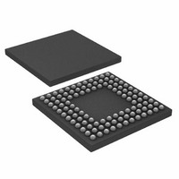
... OUTLINE DIMENSIONS BALL A1 PAD CORNER * 1.40 MAX ORDERING GUIDE 1 Model Temperature Range ADuC7122BBCZ −10°C to +95°C ADuC7122BBCZ-RL −10°C to +95° RoHS Compliant Part. 7.10 7. 5.50 BSC SQ 0.50 BSC TOP VIEW DETAIL A DETAIL A 0.15 MIN 0.35 0.30 0.25 ...
Page 94
ADuC7122 NOTES Rev Page ...
Page 95
NOTES Rev Page ADuC7122 ...
Page 96
ADuC7122 NOTES refers to a communications protocol originally developed by Philips Semiconductors (now NXP Semiconductors). ©2010 Analog Devices, Inc. All rights reserved. Trademarks and registered trademarks are the property of their respective owners. D08755-0-4/10(0) Rev ...