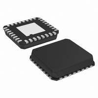
ADUC7061BCPZ32-RL Analog Devices Inc, ADUC7061BCPZ32-RL Datasheet - Page 63

ADUC7061BCPZ32-RL
Manufacturer Part Number
ADUC7061BCPZ32-RL
Description
DUAL 24-BIT AFE AND ARM 7 I.C
Manufacturer
Analog Devices Inc
Series
MicroConverter® ADuC7xxxr
Datasheet
1.EVAL-ADUC7061MKZ.pdf
(108 pages)
Specifications of ADUC7061BCPZ32-RL
Design Resources
USB Based Temperature Monitor Using ADuC7061 and an External RTD (CN0075) 4 mA-to-20 mA Loop-Powered Temperature Monitor Using ADuC7060/1 (CN0145)
Core Processor
ARM7
Core Size
16/32-Bit
Speed
10MHz
Connectivity
I²C, SPI, UART/USART
Peripherals
POR, PWM, Temp Sensor, WDT
Number Of I /o
8
Program Memory Size
32KB (32K x 8)
Program Memory Type
FLASH
Ram Size
4K x 8
Voltage - Supply (vcc/vdd)
2.375 V ~ 2.625 V
Data Converters
A/D 5x24b, 8x24b, D/A 1x14b
Oscillator Type
Internal
Operating Temperature
-40°C ~ 125°C
Package / Case
32-LFCSP
Lead Free Status / RoHS Status
Lead free / RoHS Compliant
Eeprom Size
-
Lead Free Status / RoHS Status
Lead free / RoHS Compliant
FIQSTAN
If IRQCONN[1] is asserted and FIQVEC is read, then one of
these bits asserts. The bit that asserts depends on the priority of
the FIQ. If the FIQ is of Priority 0, Bit 0 asserts; Priority 1, Bit 1
asserts; and so forth.
When a bit is set in this register, all interrupts of that priority
and lower are blocked.
To clear a bit in this register, all bits of a higher priority must be
cleared first. It is possible to clear only one bit as a time. For
example, if this register is set to 0x09, writing 0xFF changes the
register to 0x08, and writing 0xFF a second time changes the
register to 0x00.
FIQSTAN Register
Name:
Address:
Default value:
Access:
Table 75. FIQSTAN MMR Bit Designations
Bit
31:8
7:0
Table 76. IRQCONE MMR Bit Designations
Bit
31:8
7:6
5:4
3:2
1:0
Name
Reserved
Name
Reserved
IRQ3SRC[1:0]
IRQ2SRC[1:0]
IRQ1SRC[1:0]
IRQ0SRC[1:0]
FIQSTAN
0xFFFF013C
0x00000000
Read and write
Description
These bits are reserved and should not be
written to.
Setting this bit to 1 enables nesting of FIQ
interrupts. Clearing this bit means no nesting
or prioritization of FIQs is allowed.
Description
These bits are reserved and should not be written to.
[11] = External IRQ3 triggers on falling edge.
[10] = External IRQ3 triggers on rising edge.
[01] = External IRQ3 triggers on low level.
[00] = External IRQ3 triggers on high level.
[11] = External IRQ2 triggers on falling edge.
[10] = External IRQ2 triggers on rising edge.
[01] = External IRQ2 triggers on low level.
[00] = External IRQ2 triggers on high level.
[11] = External IRQ1 triggers on falling edge.
[10] = External IRQ1 triggers on rising edge.
[01] = External IRQ1 triggers on low level.
[00] = External IRQ1 triggers on high level.
[11] = External IRQ0 triggers on falling edge.
[10] = External IRQ0 triggers on rising edge.
[01] = External IRQ0 triggers on low level.
[00] = External IRQ0 triggers on high level.
Rev. B | Page 63 of 108
External Interrupts (IRQ0 to IRQ3)
The ADuC706x provides up to four external interrupt sources.
These external interrupts can be individually configured as level
triggered or rising/falling edge triggered.
To enable the external interrupt source, the appropriate bit must
first be set in the FIQEN or IRQEN register. To select the
required edge or level to trigger on, the IRQCONE register
must be appropriately configured.
To properly clear an edge based external IRQ interrupt, set the
appropriate bit in the IRQCLRE register.
IRQCONE Register
Name:
Address:
Default value:
Access:
IRQCONE
0xFFFF0034
0x00000000
Read and write
ADuC7060/ADuC7061


