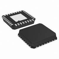
ADUC7061BCPZ32-RL Analog Devices Inc, ADUC7061BCPZ32-RL Datasheet - Page 100

ADUC7061BCPZ32-RL
Manufacturer Part Number
ADUC7061BCPZ32-RL
Description
DUAL 24-BIT AFE AND ARM 7 I.C
Manufacturer
Analog Devices Inc
Series
MicroConverter® ADuC7xxxr
Datasheet
1.EVAL-ADUC7061MKZ.pdf
(108 pages)
Specifications of ADUC7061BCPZ32-RL
Design Resources
USB Based Temperature Monitor Using ADuC7061 and an External RTD (CN0075) 4 mA-to-20 mA Loop-Powered Temperature Monitor Using ADuC7060/1 (CN0145)
Core Processor
ARM7
Core Size
16/32-Bit
Speed
10MHz
Connectivity
I²C, SPI, UART/USART
Peripherals
POR, PWM, Temp Sensor, WDT
Number Of I /o
8
Program Memory Size
32KB (32K x 8)
Program Memory Type
FLASH
Ram Size
4K x 8
Voltage - Supply (vcc/vdd)
2.375 V ~ 2.625 V
Data Converters
A/D 5x24b, 8x24b, D/A 1x14b
Oscillator Type
Internal
Operating Temperature
-40°C ~ 125°C
Package / Case
32-LFCSP
Lead Free Status / RoHS Status
Lead free / RoHS Compliant
Eeprom Size
-
Lead Free Status / RoHS Status
Lead free / RoHS Compliant
ADuC7060/ADuC7061
GENERAL-PURPOSE I/O
The ADuC706x features up to 16 general-purpose bidirectional
input/output (GPIO) pins. In general, many of the GPIO pins have
multiple functions that are configurable by user code. By default,
the GPIO pins are configured in GPIO mode. All GPIO pins have
an internal pull-up resistor with a drive capability of 1.6 mA.
All I/O pins are 3.3 V tolerant, meaning that the GPIOs support
an input voltage of 3.3 V.
Table 108. GPIO Multifunction Pin Descriptions
Port
0
1
2
GPxCON REGISTERS
GPxCON are the Port x (where x is 0, 1, or 2) control registers, which select the function of each pin of Port x as described in Table 110.
Table 109. GPxCON Registers
Name
GP0CON0
GP1CON
GP2CON
Pin Mnemonic
P0.0/SS
P0.1/SCLK/SCL
P0.2/MISO
P0.3/MOSI/SDA
P0.4/IRQ0/PWM1
P0.5/CTS
P0.6/RTS
P1.0/IRQ1/SIN/T0
P1.1/SOUT
P1.2/SYNC
P1.3/TRIP
P1.4/PWM2
P1.5/PWM3
P1.6/PWM4
P2.0/IRQ2/PWM0/EXTCLK
P2.1/IRQ3/PWM5
Address
0xFFFF0D00
0xFFFF0D04
0xFFFF0D08
00
GPIO
GPIO
GPIO
GPIO
GPIO/IRQ0
GPIO
GPIO
GPIO/IRQ1
GPIO
GPIO
GPIO
GPIO
GPIO/IRQ3
GPIO
GPIO/IRQ2/EXTCLK
GPIO/IRQ3
Configuration via GPxCON Including GP0CON0
Rev. B | Page 100 of 108
01
SS (SPI slave select).
SCLK/SCL (serial clock/SPI clock).
MISO (SPI—master in/slave out).
MOSI (SPI—master out/slave in).
PWM1 (PWM Output 1).
CTS. UART clear to send pin.
RTS. UART request to send pin.
SIN (serial input).
SOUT (serial output).
PWM sync (PWM sync input pin).
PWM trip (PWM trip input pin).
PWM2 (PWM Output 2).
PWM3 (PWM Output 3).
PWM4 (PWM Output 4).
PWM0 (PWM Output 0).
PWM5 (PWM Output 5).
Default Value
0x00000000
0x00000000
0x00000000
When the ADuC706x enters power-saving mode, the GPIO
pins retain their state.
The GPIO pins are grouped into three port buses.
Table 108 lists all the GPIO pins and their alternative functions.
A GPIO pin alternative function can be selected by writing to
the correct bits of the GPxCON register.
Access
R/W
R/W
R/W


