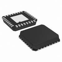
ADUC7061BCPZ32-RL Analog Devices Inc, ADUC7061BCPZ32-RL Datasheet - Page 102

ADUC7061BCPZ32-RL
Manufacturer Part Number
ADUC7061BCPZ32-RL
Description
DUAL 24-BIT AFE AND ARM 7 I.C
Manufacturer
Analog Devices Inc
Series
MicroConverter® ADuC7xxxr
Datasheet
1.EVAL-ADUC7061MKZ.pdf
(108 pages)
Specifications of ADUC7061BCPZ32-RL
Design Resources
USB Based Temperature Monitor Using ADuC7061 and an External RTD (CN0075) 4 mA-to-20 mA Loop-Powered Temperature Monitor Using ADuC7060/1 (CN0145)
Core Processor
ARM7
Core Size
16/32-Bit
Speed
10MHz
Connectivity
I²C, SPI, UART/USART
Peripherals
POR, PWM, Temp Sensor, WDT
Number Of I /o
8
Program Memory Size
32KB (32K x 8)
Program Memory Type
FLASH
Ram Size
4K x 8
Voltage - Supply (vcc/vdd)
2.375 V ~ 2.625 V
Data Converters
A/D 5x24b, 8x24b, D/A 1x14b
Oscillator Type
Internal
Operating Temperature
-40°C ~ 125°C
Package / Case
32-LFCSP
Lead Free Status / RoHS Status
Lead free / RoHS Compliant
Eeprom Size
-
Lead Free Status / RoHS Status
Lead free / RoHS Compliant
Bit
31:15
23:16
15:8
7:0
ADuC7060/ADuC7061
Table 118. GPxPAR MMR Bit Designations
GP0CON1 Control Registers
The GP0CON1 write values are as follows: GP0KEY1 = 0x7,
GP0CON1 = user value, and GP0KEY2 = 0x13.
Name:
Address:
Default value:
Access:
Function:
Table 119. GP0CON1 Write Sequence
Name
GP0KEY1
GP0CON1
GP0KEY2
Name
GPL[7:0]
GPDS[7:0]
GPPD[7:0]
GP0CON1
0xFFFF0468
0x00
Read and write
This register controls the P0.0, P0.1, P0.2, and
P0.3 functionality of the multifunction GPIO
pins.
Description
Reserved.
General I/O port pin functionality lock
registers.
GPL[7:0] = 0, normal operation.
GPL[7:0] = 1, for each GPIO pin, if this bit is
set, writing to the corresponding bit in
GPxCON or GPxDAT register bit has no
effect.
Drive strength configuration. This bit is
configurable.
GPDS[x] = 0, maximum source current is 2 mA.
GPDS[x] = 1, maximum source current is 4 mA.
Pull-Up Disable Port x[7:0].
GPPD[x] = 0, pull-up resistor is active.
GPPD[x] = 1, pull-up resistor is disabled.
Value
0x7
User value
0x13
Rev. B | Page 102 of 108
Table 120. GP0CON1 MMR Bit Designations
Bit
7:2
1
0
Name
Address:
Default value:
Access:
Function:
Name:
Address:
Default value:
Access:
Function:
Name
Reserve
d
SPII2CS
EL
ADCSEL
GP0KEY1
0xFFFF0464
0xXXXX
Write only
When writing to GP0CON1, the value of 0x07
must be written to this register in the
instruction immediately before writing to
GP0CON1.
GP0KEY2
0xFFFF046C
0xXXXX
Write only
When writing to GP0CON1, the value of 0x13
must be written to this register in the instruction
immediately after writing to GP0CON1.
Description
These bits must always be set to 0.
This bit configures the P0.0 to P0.3 functions
in I
must be set to 0 for this bit to work.
To select the P0.0, P0.1, P0.2, and P0.3
functions in SPI mode, clear this bit to 0.
To select the P0.0, P0.1, P0.2, and P0.3
functions in I
This bit is cleared by default.
This bit configures the P0.0 to P0.3 functions
as GPIO pins or as ADC input pins.
To enable P0.0, P0.1, P0.2 and P0.3 functions
as ADC inputs, set this bit to 1.
To enable P0.0, P0.1, P0.2, and P0.3 functions
as digital I/O, clear this bit to 0.
This bit is cleared by default.
2
C or SPI mode. Note that Bit 0 of GP0CON1
2
C mode, set this bit to 1.


