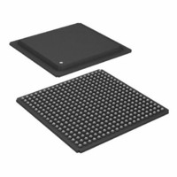
ADSP-21160NCB-100 Analog Devices Inc, ADSP-21160NCB-100 Datasheet - Page 49

ADSP-21160NCB-100
Manufacturer Part Number
ADSP-21160NCB-100
Description
IC,DSP,32-BIT,CMOS,BGA,400PIN,PLASTIC
Manufacturer
Analog Devices Inc
Series
SHARC®r
Type
Floating Pointr
Specifications of ADSP-21160NCB-100
Rohs Status
RoHS non-compliant
Interface
Host Interface, Link Port, Serial Port
Clock Rate
100MHz
Non-volatile Memory
External
On-chip Ram
512kB
Voltage - I/o
3.30V
Voltage - Core
1.90V
Operating Temperature
-40°C ~ 100°C
Mounting Type
Surface Mount
Package / Case
400-BGA
Package
400BGA
Numeric And Arithmetic Format
Floating-Point
Maximum Speed
100 MHz
Ram Size
512 KB
Device Million Instructions Per Second
100 MIPS
Lead Free Status / RoHS Status
Available stocks
Company
Part Number
Manufacturer
Quantity
Price
Company:
Part Number:
ADSP-21160NCB-100
Manufacturer:
Analog Devices Inc
Quantity:
10 000
Output Enable Time
Output pins are considered to be enabled when they have made
a transition from a high impedance state to when they start driv-
ing. The output enable time t
reference signal reaches a high or low voltage level to when the
output has reached a specified high or low trip point, as shown
in the output enable/disable diagram
pins (such as the data bus) are enabled, the measurement value
is that of the first pin to start driving.
Example System Hold Time Calculation
To determine the data output hold time in a particular system,
first calculate t
to be the difference between the ADSP-21160x DSP’s output
voltage and the input threshold for the device requiring the hold
time. A typical ΔV will be 0.4 V. C
(per data line), and I
(per data line). The hold time will be t
disable time (i.e., t
Figure 33. Voltage Reference Levels for AC Measurements (Except Output
Figure 32. Equivalent Device Loading for AC Measurements (Includes All
OUTPUT
PIN
TO
OUTPUT
INPUT
OR
DECAY
DATRWH
using the equation given above. Choose ΔV
L
1.5V
is the total leakage or three-state current
Enable/Disable)
for the write cycle).
30pF
Fixtures)
ENA
is the interval from when a
L
is the total bus capacitance
50
(Figure
DECAY
1.5V
plus the minimum
31). If multiple
Rev. B | Page 49 of 60 | February 2010
1.5V
Capacitive Loading
Output delays and holds are based on standard capacitive loads:
30 pF on all pins (see
and
tance.
delays and holds vary with load capacitance. (Note that this
graph or derating does not apply to output disable delays; see
Output Disable Time on Page
Figure
not be linear outside the ranges shown.
Figure 34. ADSP-21160M Typical Output Rise Time (10%–90%, V
Figure 35. ADSP-21160M Typical Output Rise Time (10%–90%, V
Figure 38
Figure 36
38,
25
20
15
10
30
25
20
15
10
Figure
5
0
5
0
0
0
show how output rise time varies with capaci-
and
ADSP-21160M/ADSP-21160N
39,
LOAD CAPACITANCE – pF
Figure 39
50
50
Figure
Figure
vs. Load Capacitance
vs. Load Capacitance
Y = 0.086687X
Y = 0.0813x
LOAD CAPACITANCE – pF
32).
40,
100
100
48.) The graphs of
graphically show how output
Figure
Figure
Y = 0.072781X
Y = 0.0834x
+ 2.312
+ 2.18
RISE TIME
TBD
RISE TIME
41, and
FALL TIME
FALL TIME
34,
150
150
+ 1.0653
Figure
+ 1.99
Figure 42
200
200
Figure
35,
Figure
DDEXT
DDEXT
37,
may
= Max)
250
= Min)
37,


