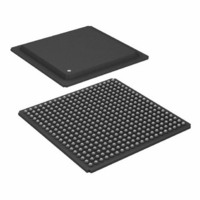
ADSP-21160NCB-100 Analog Devices Inc, ADSP-21160NCB-100 Datasheet - Page 12

ADSP-21160NCB-100
Manufacturer Part Number
ADSP-21160NCB-100
Description
IC,DSP,32-BIT,CMOS,BGA,400PIN,PLASTIC
Manufacturer
Analog Devices Inc
Series
SHARC®r
Type
Floating Pointr
Specifications of ADSP-21160NCB-100
Rohs Status
RoHS non-compliant
Interface
Host Interface, Link Port, Serial Port
Clock Rate
100MHz
Non-volatile Memory
External
On-chip Ram
512kB
Voltage - I/o
3.30V
Voltage - Core
1.90V
Operating Temperature
-40°C ~ 100°C
Mounting Type
Surface Mount
Package / Case
400-BGA
Package
400BGA
Numeric And Arithmetic Format
Floating-Point
Maximum Speed
100 MHz
Ram Size
512 KB
Device Million Instructions Per Second
100 MIPS
Lead Free Status / RoHS Status
Available stocks
Company
Part Number
Manufacturer
Quantity
Price
Company:
Part Number:
ADSP-21160NCB-100
Manufacturer:
Analog Devices Inc
Quantity:
10 000
ADSP-21160M/ADSP-21160N
Table 3. Pin Function Descriptions (Continued)
Pin
PAGE
BRST
ACK
SBTS
IRQ2–0
FLAG3–0
TIMEXP
HBR
HBG
CS
REDY
DMAR1
DMAR2
Type
O/T
I/O/T
I/O/S
I/S
I/A
I/O/A
O
I/A
I/O
I/A
O (O/D)
I/A
I/A
Function
DRAM Page Boundary. The processor asserts this pin to an external DRAM controller, to signal that
an external DRAM page boundary has been crossed. DRAM page size must be defined in the
processor’s memory control register (WAIT). DRAM can only be implemented in external memory
Bank 0; the PAGE signal can only be activated for Bank 0 accesses. In a multiprocessing system, PAGE
is output by the bus master. A keeper latch on the DSP’s PAGE pin maintains the output at the level
it was last driven (only enabled on the processor with ID2–0 = 00x).
Sequential Burst Access. BRST is asserted by ADSP-21160x or a host to indicate that data associated
with consecutive addresses is being read or written. A slave device samples the initial address and
increments an internal address counter after each transfer. The incremented address is not
pipelined on the bus. If the burst access is a read from the host to the processor, the
processor automatically increments the address as long as BRST is asserted. BRST is asserted after
the initial access of a burst transfer. It is asserted for every cycle after that, except for the last data
request cycle (denoted by RDx or WRx asserted and BRST negated). A keeper latch on the DSP’s
BRST pin maintains the input at the level it was last driven (only enabled on the processor with
ID2–0 = 00x).
Memory Acknowledge. External devices can deassert ACK (low) to add wait states to an external
memory access. ACK is used by I/O devices, memory controllers, or other peripherals to hold off
completion of an external memory access. The ADSP-21160x deasserts ACK as an output to add
wait states to a synchronous access of its internal memory, by a synchronous host or another DSP
in a multiprocessor configuration. ACK has a 2 kΩ internal pull-up resistor that is enabled on the
processor with ID2–0 = 00x.
Suspend Bus and Three-State. External devices can assert SBTS (low) to place the external bus
address, data, selects, and strobes in a high-impedance state for the following cycle. If the
ADSP-21160x attempts to access external memory while SBTS is asserted, the processor will halt
and the memory access will not be completed until SBTS is deasserted. SBTS should only be used
to recover from host processor and/or ADSP-21160x deadlock or used with a DRAM controller.
Interrupt Request Lines. These are sampled on the rising edge of CLKIN and may be either edge-
triggered or level-sensitive.
Flag Pins. Each is configured via control bits as either an input or output. As an input, it can be tested
as a condition. As an output, it can be used to signal external peripherals.
Timer Expired. Asserted for four processor core clock (CCLK) cycles when the timer is enabled and
TCOUNT decrements to zero.
Host Bus Request. Must be asserted by a host processor to request control of the
ADSP-21160x DSP’s external bus. When HBR is asserted in a multiprocessing system, the processor
that is bus master will relinquish the bus and assert HBG. To relinquish the bus, the processor places
the address, data, select, and strobe lines in a high-impedance state. HBR has priority over all
processor bus requests (BR6–1) in a multiprocessing system.
Host Bus Grant. Acknowledges an HBR bus request, indicating that the host processor may take
control of the external bus. HBG is asserted (held low) by the ADSP-21160x until HBR is released. In
a multiprocessing system, HBG is output by the processor bus master and is monitored by all others.
After HBR is asserted, and before HBG is given, HBG will float for 1 t
(1 CLKIN cycle). To avoid erroneous grants, HBG should be pulled up with a 20 kΩ to 50 kΩ external
resistor.
Chip Select. Asserted by host processor to select the ADSP-21160x, for asynchronous transfer
protocol.
Host Bus Acknowledge. The ADSP-21160x deasserts REDY (low) to add wait states to an
asynchronous host access when CS and HBR inputs are asserted.
DMA Request 1 (DMA Channel 11). Asserted by external port devices to request DMA services.
DMAR1 has a 20 kΩ internal pull-up resistor that is enabled on the ADSP-21160x with ID2–0 = 00x.
DMA Request 2 (DMA Channel 12). Asserted by external port devices to request DMA services.
DMAR2 has a 20 kΩ internal pull-up resistor that is enabled on the ADSP-21160x with ID2–0 = 00x.
Rev. B | Page 12 of 60 | February 2010
CLK


