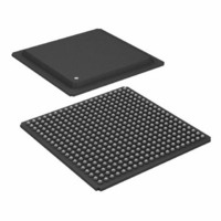
ADSP-21160NCB-100 Analog Devices Inc, ADSP-21160NCB-100 Datasheet - Page 18

ADSP-21160NCB-100
Manufacturer Part Number
ADSP-21160NCB-100
Description
IC,DSP,32-BIT,CMOS,BGA,400PIN,PLASTIC
Manufacturer
Analog Devices Inc
Series
SHARC®r
Type
Floating Pointr
Specifications of ADSP-21160NCB-100
Rohs Status
RoHS non-compliant
Interface
Host Interface, Link Port, Serial Port
Clock Rate
100MHz
Non-volatile Memory
External
On-chip Ram
512kB
Voltage - I/o
3.30V
Voltage - Core
1.90V
Operating Temperature
-40°C ~ 100°C
Mounting Type
Surface Mount
Package / Case
400-BGA
Package
400BGA
Numeric And Arithmetic Format
Floating-Point
Maximum Speed
100 MHz
Ram Size
512 KB
Device Million Instructions Per Second
100 MIPS
Lead Free Status / RoHS Status
Available stocks
Company
Part Number
Manufacturer
Quantity
Price
Company:
Part Number:
ADSP-21160NCB-100
Manufacturer:
Analog Devices Inc
Quantity:
10 000
ADSP-21160M/ADSP-21160N
ELECTRICAL CHARACTERISTICS—ADSP-21160N
Table 8
ifications are subject to change without notification.
Table 8. Electrical Characteristics—ADSP-21160N
1
2
3
4
5
6
7
8
9
10
11
12
13
14
15
16
17
18
19
20
Parameter
V
V
I
I
I
I
I
I
I
I
I
I
I
I
I
I
I
I
I
I
I
I
I
AI
C
Applies to output and bidirectional pins: DATA63–0, ADDR31–0, MS3–0, RDx, WRx, PAGE, CLKOUT, ACK, FLAG3–0, TIMEXP, HBG, REDY, DMAG1, DMAG2, BR6–1,
See Output Drive Currents
Applies to input pins: SBTS, IRQ2–0, HBR, CS, ID2–0, RPBA, EBOOT, LBOOT, CLKIN, RESET, TCK, and CLK_CFG3-0.
Applies to input pins with internal pull-ups: DR0, and DR1.
Applies to input pins with internal pull-ups: DMARx, TMS, TDI, and TRST.
Applies to CLKIN only.
Applies to all pins with keeper latches: ADDR31–0, DATA63–0, PAGE, BRST, and CLKOUT.
Current required to switch from kept high to low, or from kept low to high.
Characterized, but not tested.
Applies to three-statable pins: DATA63–0, ADDR31–0, PAGE, CLKOUT, ACK, FLAG3–0, REDY, HBG, BMS, BR6–1, TFSx, RFSx, and TDO.
Applies to three-statable pins with internal pull-ups: DTx, TCLKx, RCLKx, and EMU.
Applies to three-statable pins with internal pull-ups: MS3–0,RDx, WRx, DMAGx, PA, and CIF.
Applies to three-statable pins with internal pull-downs: LxDAT7–0, LxCLK, and LxACK.
Applies to ACK pulled up internally with 2 kΩ during reset or ID2–0 = 00x.
The test program used to measure I
I
I
Idle denotes ADSP-21160N state during execution of IDLE instruction. For more information, see
Applies to all signal pins.
Guaranteed, but not tested.
IH
IL
IHC
ILC
IKH
IKL
IKH-OD
IKL-OD
ILPU1
ILPU2
OZH
OZL
OZHPD
OZLPU1
OZLPU2
OZHA
OZLA
DD-INPEAK
DD-INHIGH
DD-INLOW
DD-IDLE
PA, BRST, CIF, DT0, DT1, TCLK0, TCLK1, RCLK0, RCLK1, TFS0, TFS1, RFS0, RFS1, LxDAT7–0, LxCLK, LxACK, BMS, TDO, and EMU.
measurements made using typical applications are less than specified. For more information, see
DD-INHIGH
DD-INLOW
OH
OL
IN
DD
shows the electrical characteristics. Note that these spec-
is a composite average based on a range of low activity code. For more information, see
is a composite average based on a range of high activity code. For more information, see
High Level Output Voltage
Low Level Output Voltage
High Level Input Current
Low Level Input Current
CLKIN High Level Input Current
CLKIN Low Level Input Current
Keeper High Load Current
Keeper Low Load Current
Keeper High Overdrive Current
Keeper Low Overdrive Current
Low Level Input Current Pull-Up1
Low Level Input Current Pull-Up2
Three-State Leakage Current
Three-State Leakage Current
Three-State Leakage Current Pull-Down
Three-State Leakage Current Pull-Up1
Three-State Leakage Current Pull-Up2
Three-State Leakage Current
Three-State Leakage Current
Supply Current (Internal)
Supply Current (Internal)
Supply Current (Internal)
Supply Current (Idle)
Supply Current (Analog)
Input Capacitance
47
for typical drive current capabilities.
DD-INPEAK
19, 20
18
represents worst-case processor operation and is not sustainable under normal application conditions. Actual internal power
3
9
3, 4, 5
15
16
17
7
1
7
1
10, 11, 12, 13
10
14
14
7, 8, 9
6
7, 8, 9
6
4
5
Rev. B | Page 18 of 60 | February 2010
11
12
13
Test Conditions
@ V
@ V
@ V
@ V
@ V
@ V
@ V
@ V
@ V
@ V
@ V
@ V
@ V
@ V
@ V
@ V
@ V
@ V
@ V
t
t
t
t
@AV
f
CCLK
CCLK
CCLK
CCLK
IN
=1 MHz, T
DDEXT
DDEXT
DDEXT
DDEXT
DDEXT
DDEXT
DDEXT
DDEXT
DDEXT
DDEXT
DDEXT
DDEXT
DDEXT
DDEXT
DDEXT
DDEXT
DDEXT
DDEXT
DDEXT
=10.0 ns, V
=10.0 ns, V
=10.0 ns, V
=10.0 ns, V
DD
=Max
=Max, V
= Max, V
= Max, V
= Max, V
= Max, V
= Max
= Max
=Min, I
=Min, I
=Max, V
=Max, V
=Max, V
=Max, V
=Max, V
=Max, V
=Max, V
=Max, V
=Max, V
=Max, V
CASE
DDINT
DDINT
DDINT
DDINT
OH
OL
Power Dissipation on Page
=25°C, V
Power Dissipation on Page
IN
IN
IN
IN
IN
IN
IN
IN
IN
IN
IN
IN
IN
IN
IN
Power Dissipation on Page
Power Dissipation on Page
=4.0 mA
=–2.0 mA
=V
=V
=0 V
=0 V
=0 V
=0 V
=V
=0 V
=0 V
=V
=0 V
= V
= 0 V
= 2.0 V
= 0.8 V
=Max
=Max
=Max
=Max
DD
DD
DD
DD
DDEXT
Max
Max
Max
Max
IN
2
=2.5 V
Max
2
47.
47.
47.
47.
Min
2.4
–250
50
–300
300
Max
0.4
10
10
25
25
–50
200
250
500
10
10
250
250
500
25
4
960
715
550
450
10
4.7
Unit
V
V
μA
μA
μA
μA
μA
μA
μA
μA
μA
μA
μA
μA
μA
μA
μA
μA
mA
mA
mA
mA
mA
mA
pF


