AD9910BSVZ-REEL Analog Devices Inc, AD9910BSVZ-REEL Datasheet - Page 56
AD9910BSVZ-REEL
Manufacturer Part Number
AD9910BSVZ-REEL
Description
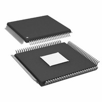
IC,FREQUENCY SYNTHESIZER,CMOS,TQFP,100PIN,PLASTIC
Manufacturer
Analog Devices Inc
Datasheet
1.AD9910BSVZ-REEL.pdf
(64 pages)
Specifications of AD9910BSVZ-REEL
Design Resources
Synchronizing Multiple AD9910 1 GSPS Direct Digital Synthesizers (CN0121)
Resolution (bits)
14 b
Master Fclk
1GHz
Tuning Word Width (bits)
32 b
Voltage - Supply
1.8V, 3.3V
Operating Temperature
-40°C ~ 85°C
Mounting Type
Surface Mount
Package / Case
100-TQFP Exposed Pad, 100-eTQFP, 100-HTQFP, 100-VQFP
Lead Free Status / RoHS Status
Lead free / RoHS Compliant
For Use With
AD9910/PCBZ - BOARD EVAL FOR AD9910 1GSPS
Lead Free Status / RoHS Status
Lead free / RoHS Compliant
Available stocks
Company
Part Number
Manufacturer
Quantity
Price
Company:

Part Number:
AD9910BSVZ-REEL
Manufacturer:
Analog Devices Inc
Quantity:
10 000


AD9910
Bit(s)
12
11
10
9
8
7
6
5
4
3
2
1
0
Mnemonic
Clear digital ramp
accumulator
Clear phase accumulator
Load ARR @ I/O update
OSK enable
Select auto OSK
Digital power-down
DAC power-down
REFCLK input power-down
Auxiliary DAC power-down
External power-down
control
Open
SDIO input only
LSB first
Description
0 = normal operation of the DRG accumulator (default).
1 = asynchronous, static reset of the DRG accumulator. The ramp accumulator remains reset
as long as this bit remains set. This bit is synchronized with either an I/O_UPDATE or a
PROFILE[2:0] change and the next rising edge of SYNC_CLK.
0 = normal operation of the DDS phase accumulator (default).
1 = asynchronous, static reset of the DDS phase accumulator.
Ineffective unless CFR1[9:8] = 11b.
The output shift keying enable bit.
Ineffective unless CFR1[9] = 1.
This bit is effective without the need for an I/O update.
0 = DAC clock signals and bias circuits are active (default).
1 = DAC clock signals and bias circuits are disabled.
This bit is effective without the need for an I/O update.
0 = auxiliary DAC clock signals and bias circuits are active (default).
1 = auxiliary DAC clock signals and bias circuits are disabled.
0 = assertion of the EXT_PWR_DWN pin affects full power-down (default).
1 = assertion of the EXT_PWR_DWN pin affects fast recovery power-down.
0 = configures the SDIO pin for bidirectional operation; 2-wire serial programming
mode (default).
1 = configures the serial data I/O pin (SDIO) as an input only pin; 3-wire serial
programming mode.
0 = configures the serial I/O port for MSB-first format (default).
1 = configures the serial I/O port for LSB-first format.
0 = OSK disabled (default).
1 = OSK enabled.
0 = manual OSK enabled (default).
1 = automatic OSK enabled.
0 = clock signals to the digital core are active (default).
1 = clock signals to the digital core are disabled.
0 = REFCLK input circuits and PLL are active (default).
1 = REFCLK input circuits and PLL are disabled.
0 = normal operation of the OSK amplitude ramp rate timer (default).
1 = OSK amplitude ramp rate timer reloaded anytime I/O_UPDATE is asserted or a
PROFILE[2:0] change occurs.
Rev. C | Page 56 of 64
Related parts for AD9910BSVZ-REEL
Image
Part Number
Description
Manufacturer
Datasheet
Request
R

Part Number:
Description:
Direct Digital Synthesis Evaluation Board
Manufacturer:
Analog Devices Inc
Datasheet:

Part Number:
Description:
3.3V CMOS Direct Digital Synthesizer
Manufacturer:
Analog Devices
Datasheet:

Part Number:
Description:
±1.7g Dual-Axis IMEMS Accelerometer Evaluation Board
Manufacturer:
Analog Devices Inc
Datasheet:

Part Number:
Description:
Inertial Sensor Evaluation System
Manufacturer:
Analog Devices Inc
Datasheet:
Part Number:
Description:
Manufacturer:
Analog Devices Inc
Datasheet:
Part Number:
Description:
Manufacturer:
Analog Devices Inc
Datasheet:
Part Number:
Description:
Manufacturer:
Analog Devices Inc
Datasheet:
Part Number:
Description:
Manufacturer:
Analog Devices Inc
Datasheet:
Part Number:
Description:
Manufacturer:
Analog Devices Inc
Datasheet:
Part Number:
Description:
Manufacturer:
Analog Devices Inc
Datasheet:
Part Number:
Description:
Manufacturer:
Analog Devices Inc
Datasheet:
Part Number:
Description:
Manufacturer:
Analog Devices Inc
Datasheet:
Part Number:
Description:
Manufacturer:
Analog Devices Inc
Datasheet: